Tuesday, October 19, 2004
Introduction
Intel has released their DDR2 motherboard in June 2004. The new generation memory, DDR2 DIMM, is officially on the market. However, this new DDR2 memory has stirred up a lot of questions. I’ve got lots of calls on "what is it?" and "how to test it?" Although the design engineers in JEDEC has been working on the DDR2 chip and DDR2 modules for a few years, yet this is the first time DDR2 modules were produced in the production environment. The production and reliability test issues has just begin to surface and there is a learning curve to be gone through by the memory module manufacturers.
CST, Inc. has been designing the DDR2 memory module tester for a year now. CST have cooperated with major system manufacturers, module manufacturers as well as memory chip manufacturers to resolve production test issues for this new type of memory. This article is an attempt to share some of the DDR2 test experience with you.
DDR vs DDR2
To enable you a better understanding, perhaps we should first look into the difference between DDR and DDR2. While DDR is powered at SSTL2.5V, DDR2 is at SSTL1.8V. This gives DDR2 an operational power, noise and speed advantage. While the power consumption might not be so important to the desktop PC, it gives the notebook PC a big lead way. Notebook computer using the DDR2 technology can now realize a longer battery life. DDR2, for speed purpose, has chosen the Ball Grid Array (BGA) package and gone from leaded chips to leadless package. There is also the Post-CAS mode that allows the data to be packed closer at the computer bus (pipeline) and thus reduce the ultimate time to access the stored data.
DDR2 New Features
Operation wise, there are DQS difference and the new ODT and OCD features. In the original DDR chip, there is one DQ strobe line for each DRAM chip. In the DDR2, the DQ strobe line has been upgraded to "differential mode". That means two lines instead of one line. This is a technique to cancel noise on the line and increase the reliability of the synchronous strobe signal. The ODT, on die termination resistor, is perhaps the best feature praised by the system board designers. It replaces the many external resistors that used to bias the output of the DDR DRAM. It practically built-in the resistors to the chip and also allows it to be programmed to several different values to suit different systems. The OCD, off chip driver mechanism, allows the flexibility of tailoring the DRAM driver strength to match the number of DIMMs and the controller characteristics in the system.
DDR2 Less Margin for Error
As we migrate to DDR2, we also found that the higher frequency is giving the system less margin and more struggle for performance. The theoretical data window has shrink to 1.5ns. in comparison to 3.7ns. In the original 266MHz DDR system. The margin will continue to reduce as the industry is moving to 800MHz and beyond data speed. More precision engineering design and calibration will have to be taken to ensure robust operations.
As frequency is getting higher, the lead frame inductance of the TSOP package becomes unacceptable. Ball grid array (BGA) package is used to replace the TSOP package and to reduce the lead inductance. This BGA package has no physical leads. It is just a solder ball contact allowing it to be attached directly to the printed circuit board.
DDR2 Mechanical Issues
Although the BGA package improves the chip performance, yet it creates tremendous problems for testing. Engineers no longer see the physically lead and no longer able to put the oscilloscope probe directly onto the pin. Instead, test probe points specifically built-in to the module will be have to be used.
Another known issue for BGA package is the mechanical solder strength. That means if the memory module is handled often, some of solder joints may come loose. Design engineers already foresee the mechanical problem. JEDEC standard has called for additional "mechanical balls" on the DRAM package. This is referring to the extra solder balls (no function balls) at the four outer corners of the BGA package. They are purely for mechanical reinforcement.
On the module level, it has 240 pin edge connection. Insertion into its mating socket will take more force than the older version of DIMM. Assuming a 1/4 Lb. per pin insertion force will amount to 60 Lbs. of insertion stress. This insertion force will not only create fatigue for the human hands, but also creates a heavy mechanical stress for the DIMM itself. Early field reports on DDR2 motherboard already indicate much higher mechanical failure of DIMM modules. The BGA package also makes it impossible to pin point the bad solder joint through visual inspection.
Traditional motherboard testing of the DIMM becomes impractical with DDR2 modules. These broken solder joint will normally cause the system not to boot and thus not allowing the system diagnostic software to point out the failing joint. Besides, a DIMM with shorted solder joints might also cause damage to the motherboard hosting the module. Besides, there are some specific conditions on the DDR2 DIMM that might not be detected by the motherboard test.
New Feature , New Problems
One of the most difficult to detect problem in the DDR2 DIMM is the ODT switch problem. Since there are multiple memory DIMM sockets on the motherboard, the system turns on only one set of ODT resistor at a time during operations. That means if two DIMMs are installed in a system, the second socket ODT might never have to be turn-on for normal operation. In this case, the second DIMM module might have a bad ODT switch and would still operate normally in the system. It is only when that DIMM is moved to the first socket that the ODT switch problem would be exposed.
The differential DQ Strobe lines have a similar problem. DDR2 DIMM standard specifies either a differential DQS mode (two lines) or a single ended DQS mode (one line) would operate in most systems. Therefore, an open DQS- line will still allow the system to work in most cases. Only when the system is stretching for the highest frequency will the fault shows up and fail the system.
When motherboard tests are not able to fully cover, functional testers will come into play with advantage. The CST SP3000-DDR2 tester is specifically designed with those failures in mind. It uses the "walk address" and "walk data" test patterns to quickly identify the address and data line shorts and opens. It also use the many level of "marching" tests to pinpoint the failed DRAM cells. It has specific "ODT" test mode as well as "DQS" test mode to identify those hard to find problems. It also has the "fault focusing" algorithm to isolate the failure to the specific DRAM chip. PC software can also be used in compliment to enhance the fault display with graphical indication of the failed chip location. For example; a address line open on one chip will be isolated to A12/U2. This gives the operator most valuable information for repair.
Another added feature of the DDR2 DIMM is the Software Write Protect (SWP). JEDEC specification dictates that every DDR2 should be software write protected on the SPD data. This SPD data is normally engraved onto the tiny EEPROM chip on the DIMM. The conventional SWP EEPROM is usually not erasable and not reversible. Due to the fact that memory module manufacturers often need to reverse their EEPROM to rewrite different contents pushed the vendors into making a new Reversible Software Write Protect (RSWP) EEPROM. This new chip allows reverse of the SWP by applying a higher voltage (10V) to initiate the reversal. The idea is to retain the SPD security on the motherboard since the motherboard will not have a 10V to reverse the SPD content. Yet a special external programmer can be used to do the RSWP. The CST SP3000-DDR2 tester not only have the normal SWP mode, it also has the RSWP feature along with the quick programming of SPD on the same single test process.
CST DDR2 Solutions
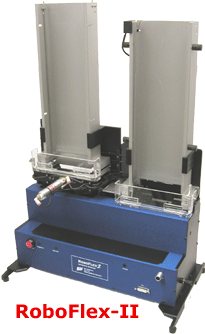
In order to reduce mechanical stress on testing, automatic test handler is also recommended. The CST RoboFlex 2 automatic DIMM handler is designed just for that. It gently receives the module from the input stack and carefully pushes it into the test socket. After the module is tested, it gently lowers the module onto the transport platform. The module is then moved to the re-stacking site. This site restacks the tested good module carefully back onto the stack.
For additional information, please visit the CST product page on www.simmtester.com
Presentation Slides from the Jedex Conference
Click to link for a brief presentation of New Challenges facing DDR2 Module Testing. A detailed article will follow soon .
By: Cecil Ho
Copyright © 2023 CST, Inc. All Rights Reserved
|