|
Clock Reference Board Navigation |
|
|
Clock Reference Board feature
A MUST for Module Manufacturers and System Designer
|
DDR Clock Reference Board Features
|
|
PC100/133 DIMM Clock Features
|
Theory of Operation
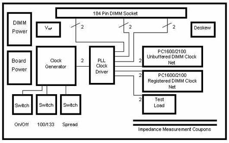
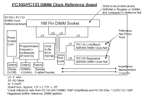
The board consists of a clock generator and a seven outputs buffer. Four of the clock signals go to the DIMM module socket while other lines goe to the on-board industry indined reference net circuit. Oscilloscope waveform meanurement is made at the DRAM and compared against the measurement at the reference net for time delay and skew.
Key Board Components
- 100/133Mhz frequency synthesizer (Philips PCK2010).
- 133Mhz 10 output low-skew clock buffer (Philips PCK2001M).
Clock Reference Nets
- 168pin PC100 unbuffered DIMM clock net (5x3.3pf loads).
- 168pin PC100/PC133 registered DIMM clock net.
- Clock buffer standard test load.
168Pin DIMM Connector
- 4 clocks wired (supports registered or unbuffered DIMMs).
- CKE, CS pins inactive, other 'registered' DIMM inputs tied low.
Switches for
- Clocks on/off
- Spread spectrum enable/disable
- 100Mhz/133Mhz frequency selection.
Electrical Characteristics
- Test board is built to norminal DIMM specifications.
- Ensures validity of clock reference net delays.
- Minimizes imdedance mismatches.
- Capacitors/resistors in test loads all set to 'norminal' spec values.
- 3.3pf for 'load capacitors (emulating PC100 SDRAM devices).
- 4pf for PLL input capacitance.
- Reference nets lifted from Intel (unbuffered) and IBM (PC133 registered) DIMM 'reference' designs - to ensure accuracy.
- Reference nets include 'via' (for DIMM socket), 'trace' (for contact), 'pad' (for DIMM tab) and 'via' (for commoning bard connection on DIMM).
Power Structure
- 2-3 power supplies required
- 3.3V (A): Vdd for 'synthesizwe' and 'buffer' chips.
- 3.3V (B): Vdd for DIMM socket (permits shmooing of DIMM under test, as a means of evaluating PLLs), or tie to 3.3V (A0.
- synthesizer decoupling includes filter networks for 3.3V supply and for clock analog supply ( some versions of this device have a unique analogy supply pin.
Board Impedance Measurement
- 5" 'coupon' available on each signal layer used for imdedance measurment.
Silkscreen Information
- Board revision (currently Rev.1)
- Probe points (unbuffered net includes labels for 2 and 3 load section).
- Probe points (unbuffered net includes labels for 2 and 3 load section).
- Switch functions.
|
