Monday, November 25, 2013
DDR4 SPD Definition
Understanding DDR4 Serial Presence Detect (SPD) Table
By: DocMemory
Introduction
Since I wrote “Understanding DDR Serial Presence Detect (SPD)
Table”
in 2003, I have been getting a lot a feedback from readers. I added
“Understanding DDR2 Serial Presence Detect (SPD) Table” in 2006. Some
of you told me that you are using these articles to train your
employees and to introduce the mysteries SPD concept to your customers.
I feel honored by your responses.
In 2007, I continued to add “Understanding DDR3 Serial
Presence
Detect (SPD) Table” to the series. Reader feedback was once again very
positive.
Lately, CST has started shipment of a DDR4 EZ Programmer.
Since the
DD4 DIMM is introduced recently, I think this is the time to add an
article for the DDR4 SPD Table. Due to the many more years of
development, the DD4 SPD table has definitely gotten more sophisticated
than the original DDR, DDR2 and DDR3 SPD table. Your attention is
required to understand and follow through. I will try to use as much
layman language as I can to accommodate you all.
Serial Presence Detect (SPD) data is probably the most
misunderstood
subject in the memory module industry. Most people only know it as the
little Eeprom device on the DIMM that often kept the module from
working properly in the computer. On the contrary, it is quite the
opposite. The SPD data actually provide vital information to the system
Bios to keep the system working in optimal condition with the memory
DIMM. This article attempts to guide you through the construction of an
SPD table with “Turbo-Tax” type of multiple choices questions. I hope
you’ll find it interesting and useful.
Byte 0
Number of Serial PD Bytes Written/ SPD Device Size/ CRC
Coverage
Bit
3 to Bit 0 describes the total size of the serial memory actually used
in the EEprom for the Serial Presence Detect data. Bit 6 to Bit 4
describes the number of bytes available in the EEprom device, usually
128byte or 256 byte. On top of that, Bit 7 indicates whether the unique
module identifier covered by the CRC encoded on bytes 126 and 127 is
based on (0-116byte) or based on (0-125byte)..
(When CST EZ-SPD
Programmer is used: Simply select items from 3 tables and automatically
calculate the final hex number)
The most common one used is:
Total SPD Bye = 512
CRC Coverage = 0-125Byte
SPD Byte used = 384 Byte
Resulting code is 23h
Byte 1
SPD Revision
Version 0.0 00h
Revision 0.7 07h
Revision 0.8
08h
Revision 0.9 09h
Revision 1.0 10h
Revision 1.1
11h
Revision 1.2 12h
Byte 2
DRAM Device Type
This refers to the DRAM type. In this case, we are only
dealing with DDR4 SDRAM.
DDR4 SDRAM: 0Ch
Byte 3
Module Type
This relates to the physical size, and category of memory
module.
Undefined 00h
RDIMM (Registered Long DIMM) 01h
UDIMM (Unbuffered Long DIMM) 02h
SODIMM (Small Outline DIMM) 03h
LRDIMM (Small Outline DIMM) 04h
Byte 4
SDRAM Density and Banks
This byte defines the total density of the DDR4 SDRAM, in
bits, and
the number of internal banks into which the memory array is divided.
Presently all DDR4 have 8 internal banks.
SDRAM Chip Size
4 Bank Groups 8 Internal Banks 4Gb 94h
4 Bank Groups 8 Internal Banks 8Gb 95h
2 Bank Groups (X16 chip) 8 Internal Banks 4Gb 54h
2 Bank Groups (X16 chip) 8 Internal Banks 8Gb 55h
Byte 5
SDRAM Addressing
This byte describes the row addressing and column addressing
in the SDRAM Device.
4Gb chips
1GbX4 16 Row X 10 Column 21h
512MbX8 15 Row X 10 Column
19h
256MbX16 15 Row X 10 Column
19h
8Gb chips
2GbX4 17 Row X 10 Column
29h
1GbX8 16 Row X 10 Column 21h
512MbX16 16 Row X 10 Column 21h
Byte 6
This byte describes the type of SDRAM Device on the module.
Monolithic single die DRAM
00h
Non-monolithic 2 die multi load stack 91h
Non-monolithic 4 die multi load stack A1h
Non-monolithic 8 die multi load stack B1h
Non-monolithic 2 die 3D stack
92h
Non-monolithic 4 die 3D stack A2h
Non-monolithic 8 die 3D stack B2h
Byte 7
SDRAM Optional Features
This byte defines support for certain SDRAM features. This
value comes from the DDR4 SDRAM data sheet.
(When CST EZ-SPD
Programmer is used: Simply select the tMAW and the MAC. It
automatically calculate final hex number for you)
Maximum Activate Window = tMAW
Maximum Ativate Count = tRRMAC
| tMAW
= 8192 * tREFI, with tRRMAC =
700K |
01h |
| tMAW = 8192 * tREFI,
with tRRMAC = 600K |
02h |
| tMAW = 8192 * tREFI,
with tRRMAC = 500K |
03h |
| tMAW = 8192 * tREFI,
with tRRMAC = 400K |
04h |
| tMAW = 8192 * tREFI,
with tRRMAC = 300K |
05h |
| |
|
| tMAW = 4096 * tREFI,
with tRRMAC = 700K |
11h |
| tMAW = 4096 * tREFI,
with tRRMAC = 600K |
12h |
| tMAW = 4096 * tREFI,
with tRRMAC = 500K |
13h |
| tMAW = 4096 * tREFI,
with tRRMAC = 400K |
14h |
| tMAW = 4096 * tREFI,
with tRRMAC = 300K |
15h |
| |
|
| tMAW = 2048 * tREFI,
with tRRMAC = 700K |
21h |
| tMAW = 2048 * tREFI,
with tRRMAC = 600K |
22h |
| tMAW = 2048 * tREFI,
with tRRMAC = 500K |
23h |
| tMAW = 2048 * tREFI,
with tRRMAC = 400K |
24h |
| tMAW
= 2048 * tREFI, with tRRMAC =
300K |
25h |
| |
|
| Optional Features Unknown |
30h |
Byte 8
SDRAM Thermal and Refresh
Options
Reserved 00h
Byte 9
Reserved
Reserved 00h
Byte 10
Reserved
Reserved 00h
Byte 11
Module Nominal Voltage, VDD
This byte describes the voltage Level for DRAM and other components
on the module such as the register or memory buffer if applicable.
However, this excludes VDDSPD.
Normal DRAM VDD=1.2V only 03h
Normal DRAM VDD =1.2V, Can endures but not operate on VDD TBD1 0Bh
Byte 12
Module Organization
This byte describes the organization of the module.
(When CST EZ-SPD
Programmer is used: Simply select number of Ranks
and Device Width. It automatically calculate final hex number)
|
1 Rank module using X8 chips
|
01h |
|
2 Rank module using X8 chips
|
09h |
|
1 Rank module using X4 chips |
00h |
|
2 Rank module using X4 chips
|
08h |
|
4 Rank module using X8 chips
|
19h |
|
4 Rank module using X4chips
|
18h |
|
1 Rank module using X16 chips
|
02h |
|
2 Rank module using X16 chips
|
0Ah |
Byte 13
Module Memory Bus Width
This refers to the primary bus width of the module plus the additional
with provided by ECC
16bit 01h
32bit 02h
64bit (no parity) 03h
64bit + ECC (72bit)
0Bh
Byte 14
Module Thermal Sensor
This byte describes the module’s supported thermal options.
Use thermal sensor 80h
Does not use thermal sensor 00h
Byte 15
Reserved
Reserved 00h
Byte 16
Reserved
Reserved 00h
Byte 17
Time bases
This byte defines a value in picoseconds that represent s the
fundamental timebase for fine grain and medium grain timing
calculations. These values are used as a multiplier for formulating
subsequent timing parameters.
Medium Timebase (MTB) of 125ps and Fine Timebase (FTB) of 1ps are
defined 00h
Byte 18
SDRAM Minimum Cycle Time (tCKAVGmin)
This byte defines the minimum cycle time for the SDRAM module, in (MTB)
units.
Based on medium timebase of 0.125ns
tCKAVGmin
DDR4
|
1600 1250ps 0Ah
|
| DDR4
|
1866 1071ps 09h
|
|
DDR4
|
2133 938ps 08h
|
|
DDR4
|
2400 833ps 07h
|
|
DDR4
|
2666 750ps 06h
|
|
DDR4
|
3200 625ps 05h
|
Byte 19
SDRAM Maximum Cycle Time (tCKAVGmax)
This byte defines the maximum cycle time for the SDRAM module,
in (MTB) units.
Based on medium timebase of 0.125ns
tCKAVGmax
DDR4
|
1600 1500ps 0Ch
|
|
DDR4
|
1866 1500ps 0Ch
|
|
DDR4
|
2133 1500ps 0Ch
|
|
DDR4
|
2400 1500ps 0Ch
|
|
DDR4
|
2666 TBDps TBDh
|
|
DDR4
|
3200 TBDps TBDh
|
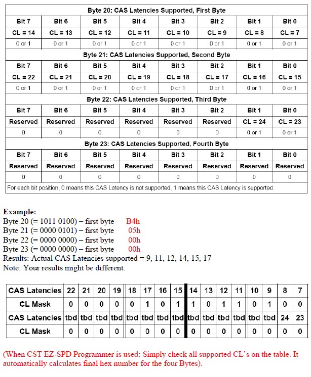
Byte 20, CAS Latencies supported (First Byte)
Byte 21, CAS Latencies supported (Second Byte)
Byte 22, CAS Latencies supported (Third Byte)
Byte 23, CAS Latencies supported (Fourth Byte)
Thesse byte define which CAS Latency (CL) values are
supported. The
range is from CL=7 through CL=24with one bit per possible CAS Latency.
Byte 24
Minimum CAS Latency Time (tAAmin)
This word defines the minimum CAS Latency in medium timebase
(MTB) units.
Based on medium timebase of 0.125ns
tAAmin
DDR4-1600J 12.5ns
|
64h |
|
DDR4-1600K 13.75ns
|
6Eh |
|
DDR4-1600Kdownbin 13.5ns
|
6Ch |
|
DDR4-1600JL 15.0ns
|
78h |
|
DDR4-1866L 12.85ns
|
67h |
|
DDR4-1866M 13.92ns
|
70h |
|
DDR4-1866M downbin 13.50ns
|
6Ch |
|
DDR4-1866N 15.00ns
|
78h |
|
DDR4-2133N 13.13ns
|
6Ah |
|
DDR4-2133P 14.06ns
|
71h |
|
DDR4-2133Pdownbin 12.50ns
|
6Ch |
|
DDR4-2133R 15.00ns
|
78h |
| DDR4-2400P 12.50ns
|
64h |
| DDR4-2400R 13.32ns
|
6Bh |
| DDR4-2400U 15.00ns
|
78h |
| DDR4-2666 |
tbd |
| DDR4-3200 |
tbd |
Byte 25
Minimum RAS to CAS delay Time (tRCDmin)
This word defines the minimum SDRAM RAS to CAS delay Time in
medium timebase (MTB) units.
Based on fine timebase of 0.125ns
tRCDmin
DDR4-1600J 12.5ns
|
64h |
|
DDR4-1600K 13.75ns
|
6Eh |
| DDR4-1600Kdownbin 13.5ns
|
6Ch |
|
DDR4-1600JL 15.0ns
|
78h |
|
DDR4-1866L 12.85ns
|
67h |
|
DDR4-1866M 13.92ns
|
70h |
|
DDR4-1866M downbin 13.50ns
|
6Ch |
|
DDR4-1866N 15.00ns
|
78h |
|
DDR4-2133N 13.13ns
|
6Ah |
|
DDR4-2133P 14.06ns
|
71h |
|
DDR4-2133Pdownbin 12.50ns
|
6Ch |
|
DDR4-2133R 15.00ns
|
78h |
| DDR4-2400P 12.50ns
|
64h |
| DDR4-2400R 13.32ns
|
6Bh |
| DDR4-2400U 15.00ns
|
78h |
| DDR4-2666 |
tbd |
| DDR4-3200 |
tbd |
Byte 26
Minimum Row Precharge Delay Time (tRPmin)
This word defines the minimum SDRAM Row Precharge Delay Time
in medium timebase (MTB)units
Based on medium timebase of 0.125ns
tRPmin
DDR4-1600J 12.5ns
|
64h |
|
DDR4-1600K 13.75ns
|
6Eh |
|
DDR4-1600Kdownbin 13.5ns
|
6Ch |
|
DDR4-1600JL 15.0ns
|
78h |
|
DDR4-1866L 12.85ns
|
67h |
| DDR4-1866M 13.92ns
|
70h |
|
DDR4-1866M downbin 13.50ns
|
6Ch |
|
DDR4-1866N 15.00ns
|
78h |
|
DDR4-2133N 13.13ns
|
6Ah |
|
DDR4-2133P 14.06ns
|
71h |
|
DDR4-2133Pdownbin 12.50ns
|
6Ch |
|
DDR4-2133R 15.00ns
|
78h |
| DDR4-2400P 12.50ns
|
64h |
| DDR4-2400R 13.32ns
|
6Bh |
| DDR4-2400U 15.00ns
|
78h |
| DDR4-2666 |
tbd |
| DDR4-3200 |
tbd |
Byte 27
Upper Nibbles for tRASmin
and tRCmin
This byte defines the most significant nibbles for the values
of tRASmin n (byte 28) and tRCmin (byte 29).
tRCmin/ tRASmin
DDR4-1600J 47.5/35ns
|
11h |
|
DDR4-1600K 48.75/35ns
|
11h |
|
DDR4-1600Kdownbin 48.5/35ns
|
11h |
|
DDR4-1600JL 50/35ns
|
11h |
|
DDR4-1866L 46.85/34ns
|
11h |
|
DDR4-1866M 47.92/34ns
|
11h |
|
DDR4-1866M downbin 47.50/34ns
|
11h |
|
DDR4-1866N 49.00/34ns
|
11h |
|
DDR4-2133N 46.13/33ns
|
11h |
|
DDR4-2133P 47.06/33ns
|
11h |
|
DDR4-2133Pdownbin 46.50/33ns
|
11h |
|
DDR4-2133R 48.00/33ns
|
11h |
| DDR4-2400P 44.50/32ns
|
11h |
| DDR4-2400R 45.32/32ns
|
11h |
| DDR4-2400U 47.00/32ns
|
11h |
| DDR4-2666 |
tbd |
|
DDR4-3200 |
tbd |
Byte 28
Minimum Active to
Precharge Delay Time (tRASmin), Least
Significant Byte
The lower nibble of Byte 27 and the contents of Byte 28
combined
create a 12-bit value which defines the minimum SDRAM Active to
Precharge Delay Time in medium timebase (MTB) units. The most
significant bit is Bit 3 of Byte 27 and the least significant bit is
Bit 0 of Byte 28.
Based on medium timebase of 0.125ns
tRASmin
DDR4-1600 35ns
|
18h |
| |
|
|
DDR4-1866 34ns
|
10h |
| |
|
|
DDR4-2133 33ns
|
08h |
| |
|
| DDR4-2400P 32ns
|
00h |
| |
|
| DDR4-2666 tbd |
|
|
DDR4-3200 tbd |
|
Byte 29
Minimum Active to
Active/Refresh Delay Time (tRCmin), Least
Significant Byte.
The upperer nibble of Byte 27 and the contents of Byte 29
combined
create a 12-bit value which defines the minimum SDRAM Active to
Active/Refresh Delay Time in medium timebase (MTB) units. The most
significant bit is Bit 7 of Byte 27 and the least significant bit is
Bit 0 of Byte 29.
Based on medium timebase of 0.125ns
tRCmin
DDR4-1600J 47.5ns
|
7Ch |
|
DDR4-1600K 48.75ns
|
86h |
|
DDR4-1600Kdownbin 48.5ns
|
84h |
|
DDR4-1600L 50ns
|
90h |
|
DDR4-1866L 46.85ns
|
77h |
|
DDR4-1866M 47.92ns
|
80h |
|
DDR4-1866M downbin 47.50ns
|
7Ch |
|
DDR4-1866N 49ns
|
88h |
|
DDR4-2133N 46.13ns
|
72h |
|
DDR4-2133P 47.06ns
|
79h |
|
DDR4-2133Pdownbin 46.50ns
|
74h |
|
DDR4-2133R 48.00ns
|
80h |
| DDR4-2400P 44.50ns
|
64h |
| DDR4-2400R 45.32ns
|
6Bh |
| DDR4-2400U 47.00ns
|
78h |
| DDR4-2666 tbd |
|
| DDR4-3200 tbd |
|
Byte 30 Minimum Refresh
Recovery Delay time (tRFC1min), LSB
Byte 31 Minimum Refresh Recovery Delay time (tRFC1min), MSB
This word defines the minimum SDRAM Refresh Recovery Delay
Time in
Minimum Timebase (MTB) units. This value is read off the data sheet.
Based on medium timebase of 0.125ns
tRFC1min
4Gb DDR4 260ns Byte 30 (LSB) = 20h
Byte 31 (MSB) =
08h
8Gb DDR4 350ns Byte 30 (LSB) =
F0h Byte 31 (MSB)=
0Ah
Byte 32 Minimum Refresh Recovery Delay time (tRFC2min), LSB
Byte 33 Minimum Refresh Recovery Delay time (tRFC2min), MSB
This word defines the minimum SDRAM Refresh Recovery Delay
Time in
Minimum Timebase (MTB) units. This value is read off the data sheet.
Based on medium timebase of 0.125ns
tRFC2min
4Gb DDR4 160ns Byte 32 (LSB) =
00h Byte 33 (MSB) =
05h
8Gb DDR4 260ns Byte 32 (LSB) =
20h Byte 33 (MSB) =
08h
Byte 34 Minimum Refresh Recovery Delay time (tRFC4min), LSB
Byte 35 Minimum Refresh Recovery Delay time (tRFC4min), MSB
This word defines the minimum SDRAM Refresh Recovery Delay
Time in
Minimum Timebase (MTB) units. This value is read off the data sheet.
Based on medium timebase of 0.125ns
tRFC4min
4Gb DDR4 110ns Byte 34 (LSB) =
70h Byte 35 (MSB) =
03h
8Gb DDR4 160ns Byte 34 (LSB) = 00h
Byte 35 (MSB) = 05h
Byte 36
Upper Nibble for tFAW
This byte defines the most significant nibble for the value of
tFAW (SPD byte 37). This value comes from the DDR4
SDRAM data sheet.
tFAW
DDR4 1600, 2KB page size Byte
36 =
|
01h |
|
DDR4 1600, 1KB page size Byte 36 =
|
00h |
|
DDR4 1600, 1/2KB page size Byte 36 =
|
00h |
|
DDR4 1866, 2KB page size Byte 36 =
|
00h |
|
DDR4 1866, 1KB page size Byte 36 =
|
00h |
|
DDR4 1866, 1/2KB page size Byte 36 =
|
00h |
|
DDR4 2133, 2KB page size Byte 36 =
|
00h |
|
DDR4 2133, 1KB page size Byte 36 =
|
00h |
|
DDR4 2133, 1/ 2KB page size Byte 36 =
|
00h |
|
DDR4 2400, 2KB page size Byte 36 =
|
00h |
|
DDR4 2400, 2KB page size Byte 36 =
|
00h |
|
DDR4 2400, 2KB page size Byte 36 =
|
00h |
Byte 37
Minimum four Activate Window Delay Time (tFAWmin),
Least Significant Byte.
The lower nibble of Byte 36 and the contents of Byte 37
combined
create a 12-bit value which defines the minimum SDRAM Four Activate
window Delay Time in medium timebase (MTB) units. This value comes from
the DDR4 SDRAM data sheet.
tFAWmin
DDR4 1600, 2KB page size
Byte 37 =
|
18h |
|
DDR4 1600, 1KB page size Byte 37 =
|
C8h |
|
DDR4 1600, 1/2KB page size Byte 37 =
|
A0h |
| DDR4 1866, 2KB page size Byte 37 =
|
F0h |
|
DDR4 1866, 1KB page size Byte 37 =
|
B8h |
|
DDR4 1866, 1/2KB page size Byte 37 =
|
88h |
|
DDR4 2133, 2KB page size Byte 37 =
|
F0h |
|
DDR4 2133, 1KB page size Byte 37 =
|
B8h |
|
DDR4 2133, 1/ 2KB page size Byte 37 =
|
88h |
|
DDR4 2400, 2KB page size Byte 37 =
|
F0h |
|
DDR4 2400, 2KB page size Byte 37 =
|
A8h |
|
DDR4 2400, 2KB page size Byte 37 = |
68h |
Byte 38
Minimum Activate to
Activate Delay Time (tRRD_Smin),different
bank group
This byte defines the minimum SDRAM Activate to Activate delay
Time
to different bank groups in medium timebase (MTB) units. This value
comes from the DDR4 SDRAM data sheet.
Based on medium timebase of 0.125ns
tRRD_Smin
DDR4 1600, 2KB page size
6.0ns
|
30h |
|
DDR4 1600, 1KB page size 5.0ns
|
28h |
|
DDR4 1600, 1/2KB page size 5.0ns
|
28h |
|
DDR4 1866, 2KB page size 5.3ns
|
2Bh |
|
DDR4 1866, 1KB page size 4.2ns
|
22h |
| DDR4 1866, 1/2KB page size
4.2ns
|
22h |
|
DDR4 2133, 2KB page size 5.3ns
|
2Bh |
|
DDR4 2133, 1KB page size 3.7ns
|
1Eh |
|
DDR4 2133, 1/ 2KB page size 3.7ns
|
1Eh |
|
DDR4 2400, 2KB page size 5.3ns
|
2Bh |
|
DDR4 2400, 2KB page size 3.3ns
|
1Bh |
|
DDR4 2400, 2KB page size 3.3ns |
1Bh |
Byte 39
Minimum Activate to
Activate Delay Time (tRRD_Lmin), same
bank group
This byte defines the minimum SDRAM Activate to Activate delay
Time
to same bank group in medium timebase (MTB) units. This value comes
from the DDR4 SDRAM data sheet.
Based on medium timebase of 0.125ns
tRRD_Smin
DDR4 1600, 2KB page size
7.5ns
|
3Ch |
|
DDR4 1600, 1KB page size 6.0ns
|
30h |
|
DDR4 1600, 1/2KB page size 6.0ns
|
30h |
|
DDR4 1866, 2KB page size 6.4ns
|
34h |
|
DDR4 1866, 1KB page size 5.3ns
|
2Bh |
|
DDR4 1866, 1/2KB page size 5.3ns
|
2Bh |
|
DDR4 2133, 2KB page size 6.4ns
|
34h |
|
DDR4 2133, 1KB page size 5.3ns
|
2Bh |
|
DDR4 2133, 1/ 2KB page size 5.3ns
|
2Bh |
|
DDR4 2400, 2KB page size 6.4 ns
|
34h |
|
DDR4 2400, 2KB page size 4.9ns
|
28h |
|
DDR4 2400, 2KB page size 4.9ns |
28h |
Byte 40
Minimum CAS to CAS Delay Time (tCCD_Lmin), same bank
group
This byte defines the minimum SDRAM CAS to CAS Delay Time to
the
same bank group in medium timebase (MTB) units. This value comes from
the DDR4 SDRAM data sheet.
Based on medium timebase of 0.125ns
tCCD_Lmin
DDR4 1600 6.250ns
|
32h |
| DDR4 1866 5.355ns
|
2Bh |
|
DDR4 2133 5.355ns
|
2Bh |
|
DDR4 2400 5.000 ns
|
28h |
Byte 41-59
Reserved, Base configuration Section
Must be coded as 00h
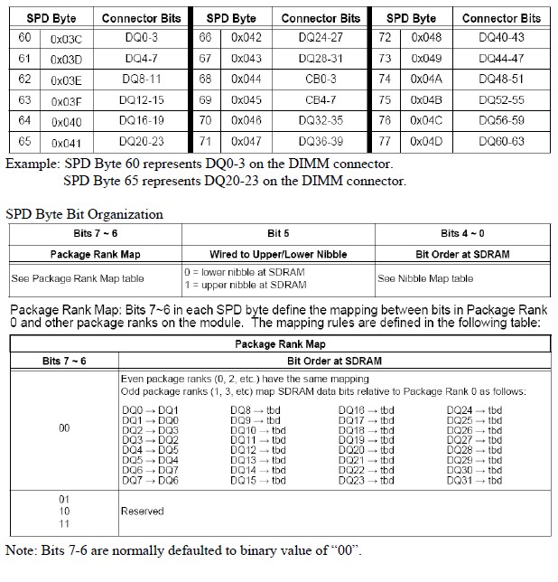
Byte 60 – 77
Connector to SDRAM Bit Mapping
DDR4 DIMM module layouts are difficult. Bit sequence at the
edge
connector of the module does not necessary match the DQ sequence at the
SDRAM. Therefore, DQ scrambling is used. These bytes describe the DQ
scrambling sequence of the particular module.
Each SPD Byte represents a DQ nibble (4 Bits)
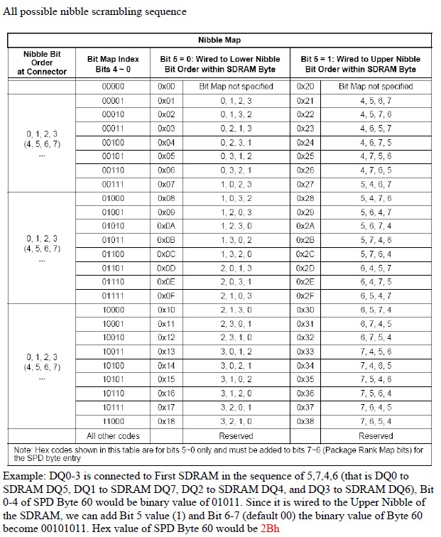
More Examples:
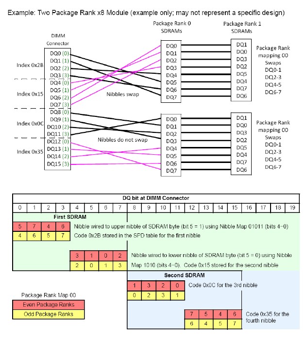
Case 1: DQ0-3 is connected to First SDRAM
in the sequence of
5,7,4,6 (that is DQ0 to SDRAM DQ5, DQ1 to SDRAM DQ7, DQ2 to SDRAM DQ4,
and DQ3 to SDRAM DQ6), Bit 0-4 of SPD Byte 60 would be binary value of
01011. Since it is wired to the Upper Nibble of the SDRAM, we can add
Bit 5 value (1) and Bit 6-7 (default 00) the binary value of Byte 60
become 00101011. Hex value of SPD Byte 60 would be 2Bh
Case 2: DQ4-7 is connected to First SDRAM
in the sequence of
3,1,0,2 (that is DQ4 to SDRAM DQ3, DQ5 to SDRAM DQ1, DQ6 to SDRAM DQ0,
and DQ7 to SDRAM DQ2), Bit 0-4 of SPD Byte 61 would be binary value of
10101. Since it is wired to the Lower Nibble of the SDRAM, we can add
Bit 5 value (0) and Bit 6-7 (default 00) the binary value of Byte 61
become 00010101. Hex value of SPD Byte 61 would be 15h
Case 3: DQ8-11 is connected to Second SDRAM
in the sequence
of 1,3,2,0 (that is DQ8 to SDRAM DQ1, DQ9 to SDRAM DQ3, DQ10 to SDRAM
DQ2, and DQ11 to SDRAM DQ0), Bit 0-4 of SPD Byte 62 would be binary
value of 01100. Since it is wired to the Lower Nibble of the SDRAM, we
can add Bit 5 value (0) and Bit 6-7 (default 00) the binary value of
Byte 62 become 00001100. Hex value of SPD Byte 62 would be 0Ch
Case 4: DQ12-15 is connected to Second
SDRAM in the sequence
of 7,5,4,6 (that is DQ12 to SDRAM DQ7, DQ13 to SDRAM DQ5, DQ14 to SDRAM
DQ4, and DQ15 to SDRAM DQ6), Bit 0-4 of SPD Byte 63 would be binary
value of 10101. Since it is wired to the Upper Nibble of the SDRAM, we
can add Bit 5 value (1) and Bit 6-7 (default 00) the binary value of
Byte 63 become 00110101. Hex value of SPD Byte 63 would be 35h
Case 5: CB0-3 is connected to Fifth SDRAM
in the sequence of
0,1,2,3 (that is CB0 to SDRAM DQ0, CB1 to SDRAM DQ1, CB2 to SDRAM DQ2,
and CB3 to SDRAM DQ3), Bit 0-4 of SPD Byte 68 would be binary value of
00001. Since it is wired to the Lower Nibble of the SDRAM, we can add
Bit 5 value (0) and Bit 6-7 (default 00) the binary value of Byte 68
become 00000001. Hex value of SPD Byte 68 would be 01h
Case 6: CB4-7 is connected to Fifth SDRAM
in the sequence of
4,5,6,7 (that is CB4 to SDRAM DQ4, CB5 to SDRAM DQ5, CB6 to SDRAM DQ26,
and CB7 to SDRAM DQ7), Bit 0-4 of SPD Byte 69 would be binary value of
00001. Since it is wired to the Upper Nibble of the SDRAM, we can add
Bit 5 value (1) and Bit 6-7 (default 00) the binary value of Byte 69
become 00100001. Hex value of SPD Byte 69 would be 21h
Byte 78 – 116
Reserved, Base Configuration Section
Must be coded with 00h
Byte 117
Fine Offset for Minimum CAS to CAS Delay Time
(tCCD_Lmin), same bank group.
This Byte modifies the calculation of SPD Byte 40 with a fine
correction using FTB units. The value of tCCD_Lmin comes from the SDRAM
data sheet. This value is a two’s complement multiplier for FTB units,
ranging from +127 to -128.
Based on Fine timebase of 0.001ns
tCCD_Lmin
DDR4 1600 6.250ns 0
|
00h |
|
DDR4 1866 5.355ns -20
|
EDh |
|
DDR4 2133 5.355ns -20
|
EDh |
|
DDR4 2400 5.000 ns 0
|
00h |
Byte 118
Fine Offset for Minimum Activate to Activate Delay Time
(tRRD_Lmin), different bank group
This byte modifies the calculation of SPD Byte 39 (MTB units)
with a
fine correction using FTB units. The value of tRRD_Lmin comes from the
SDRAM data sheet. This value is a two’s complement multiplier for FTB
ranging from +128 to -128.
Based on Fine timebase of 0.001ns
tRRD_Lmin
DDR4 1600, 2KB page size
7.50ns 0
|
00h |
|
DDR4 1600, 1KB page size 6.00ns 0
|
00h |
|
DDR4 1600, 1/2KB page size 6.00ns 0
|
00h |
|
DDR4 1866, 2KB page size 6.40ns -100
|
9Dh |
|
DDR4 1866, 1KB page size 5.30ns -75
|
B5h |
|
DDR4 1866, 1/2KB page size 5.30ns -75
|
B5h |
|
DDR4 2133, 2KB page size 6.40ns -100
|
9Dh |
|
DDR4 2133, 1KB page size 5.30ns -75
|
B5h |
|
DDR4 2133, 1/ 2KB page size 5.30ns -75
|
B5h |
| DDR4 2400, 2KB page size 6.40ns
-100
|
9Dh |
|
DDR4 2400, 2KB page size 4.90ns -100
|
9Dh |
|
DDR4 2400, 2KB page size 4.90ns -100 |
9Dh |
Byte 119
Fine Offset for Minimum Activate to Activate Delay Time
(tRRD_Smin), same bank group
This byte modifies the calculation of SPD Byte 38 (MTB units)
with a
fine correction using FTB units. The value of tRRD_Smin comes from the
SDRAM data sheet. This value is a two’s complement multiplier for FTB
ranging from +128 to -128.
Based on Fine timebase of 0.001ns
tRRD_Smin
DDR4 1600, 2KB page size
6.00ns 0
|
00h |
|
DDR4 1600, 1KB page size 5.00ns 0
|
00h |
| DDR4 1600, 1/2KB page size 5.00ns
0
|
00h |
|
DDR4 1866, 2KB page size 5.30ns -75
|
B5h |
|
DDR4 1866, 1KB page size 4.20ns -50
|
CFh |
|
DDR4 1866, 1/2KB page size 4.20ns -50
|
CFh |
|
DDR4 2133, 2KB page size 5.30ns -75
|
B5h |
|
DDR4 2133, 1KB page size 3.70ns -50
|
CFh |
|
DDR4 2133, 1/ 2KB page size 3.70ns -50
|
CFh |
|
DDR4 2400, 2KB page size 5.30ns -75
|
B5h |
|
DDR4 2400, 2KB page size 3.30ns -75
|
B5h |
|
DDR4 2400, 2KB page size 3.30ns -75
|
B5h |
Byte 120
Fine Offset for Minimum
Active to Active/Refresh Delay Time
(tRCmin)
This byte modifies the calculation of SPD Byte 27 and 29 (MTB
units)
with a fine correction using FTB units. The value of tRRD_Smin comes
from the SDRAM data sheet. This value is a two’s complement multiplier
for FTB ranging from +128 to -128.
Based on Fine timebase of 0.001ns
tRCmin
DDR4-1600J 47.50ns 0
|
00h |
|
DDR4-1600K 48.75ns 0
|
00h |
|
DDR4-1600Kdownbin 48.50ns 0
|
00h |
|
DDR4-1600L 50.00ns 0
|
00h |
|
DDR4-1866L 46.85ns -25
|
E8h |
|
DDR4-1866M 47.92ns -80
|
B1h |
|
DDR4-1866M downbin 47.50ns 0
|
00h |
|
DDR4-1866N 49.00ns 0
|
00h |
|
DDR4-2133N 46.13ns -120
|
89h |
|
DDR4-2133P 47.06ns -65
|
C0h |
|
DDR4-2133Pdownbin 46.50ns 0
|
00h |
|
DDR4-2133R 48.00ns 0
|
00h |
| DDR4-2400P 44.50ns 0
|
00h |
| DDR4-2400R 45.32ns -55
|
CAh |
| DDR4-2400U 47.00ns 0
|
00h |
| DDR4-2666 tbd |
|
| DDR4-3200 tbd |
|
Byte 121
Fine Offset for Minimum Row Precharge Delay Time
(tRPmin)
This byte modifies the calculation of SPD Byte 26 (MTB units)
with a
fine correction using FTB units. The value of tRPmin comes from the
SDRAM data sheet. This value is a two’s complement multiplier for FTB
ranging from +128 to -128.
Based on Fine timebase of 0.001ns
tRPmin
DDR4-1600J 12.5ns 0
|
00h |
|
DDR4-1600K 13.75ns 0
|
00h |
|
DDR4-1600Kdownbin 13.5ns 0
|
00h |
|
DDR4-1600JL 15.0ns 0
|
00h |
|
DDR4-1866L 12.85ns -25
|
E7h |
|
DDR4-1866M 13.92ns -80
|
B0h |
|
DDR4-1866M downbin 13.50ns 0
|
00h |
|
DDR4-1866N 15.00ns 0
|
00h |
|
DDR4-2133N 13.13ns -120
|
89h |
|
DDR4-2133P 14.06ns -65
|
C0h |
|
DDR4-2133Pdownbin 12.50ns 0
|
00h |
|
DDR4-2133R 15.00ns 0
|
00h |
| DDR4-2400P 12.50ns 0
|
00h |
| DDR4-2400R 13.32ns -55
|
CAh |
| DDR4-2400U 15.00ns 0
|
00h |
| DDR4-2666 tbd |
|
| DDR4-3200 tbd |
|
Byte 122
Fine Offset for Minimum RAS to CAS delay Time
(tRCDmin)
This byte modifies the calculation of SPD Byte 25 (MTB units)
with a
fine correction using FTB units. The value of tRCDmin comes from the
SDRAM data sheet. This value is a two’s complement multiplier for FTB
ranging from +128 to -128.
Based on Fine timebase of 0.001ns
|
tRCDmin DDR4-1600J 12.5ns 0
|
00h |
|
DDR4-1600K 13.75ns 0
|
00h |
|
DDR4-1600Kdownbin 13.5ns 0
|
00h |
|
DDR4-1600JL 15.0ns 0
|
00h |
|
DDR4-1866L 12.85ns -25
|
E7h |
|
DDR4-1866M 13.92ns -80
|
B0h |
|
DDR4-1866M downbin 13.50ns 0
|
00h |
|
DDR4-1866N 15.00ns 0
|
00h |
|
DDR4-2133N 13.13ns -120
|
89h |
|
DDR4-2133P 14.06ns -65
|
C0h |
|
DDR4-2133Pdownbin 12.50ns 0
|
00h |
| DDR4-2133R 15.00ns 0
|
00h |
| DDR4-2400P 12.50ns 0
|
00h |
| DDR4-2400R 13.32ns -55
|
CAh |
| DDR4-2400U 15.00ns 0
|
00h |
| DDR4-2666 tbd |
|
|
DDR4-3200 tbd |
|
Byte 123
Fine Offset for Minimum CAS Latency Time (tAAmin)
This byte modifies the calculation of SPD Byte 24 (MTB units)
with a
fine correction using FTB units. The value of tAAmin comes from the
SDRAM data sheet. This value is a two’s complement multiplier for FTB
ranging from +128 to -128.
Based on Fine timebase of 0.001ns
tAAmin
DDR4-1600J 12.50ns 0
|
00h |
|
DDR4-1600K 13.75ns 0
|
00h |
|
DDR4-1600Kdownbin 13.50ns 0
|
00h |
|
DDR4-1600JL 15.00ns 0
|
00h |
|
DDR4-1866L 12.85ns -25
|
E7h |
|
DDR4-1866M 13.92ns -80
|
B0h |
|
DDR4-1866M downbin 13.50ns 0
|
00h |
|
DDR4-1866N 15.00ns 0
|
00h |
| DDR4-2133N 13.13ns -120
|
89h |
|
DDR4-2133P 14.06ns -65
|
C0h |
|
DDR4-2133Pdownbin 12.50ns 0
|
00h |
|
DDR4-2133R 15.00ns 0
|
00h |
| DDR4-2400P 12.50ns 0
|
00h |
| DDR4-2400R 13.32ns -55
|
CAh |
| DDR4-2400U 15.00ns 0
|
00h |
| DDR4-2666 tbd |
|
|
DDR4-3200 tbd |
|
Byte 124
Fine Offset for SDRAM Maximum Cycle Time (tCKAVGmax)
This byte modifies the calculation of SPD Byte 19 (MTB units)
with a
fine correction using FTB units. The value of tCKAVGmax comes from the
SDRAM data sheet. This value is a two’s complement multiplier for FTB
ranging from +128 to -128.
Based on Fine timebase of 0.001ns
tCKAVGmax
DDR4-1600 0 |
00h |
|
DDR4-1866 0 |
00h |
|
DDR4-2133 0s |
00h |
|
DDR4-2400 0
|
00h |
|
DDR4-2666 TBDps |
|
|
DDR4-3200 TBDps |
|
Byte 125
Fine Offset for SDRAM Minimum Cycle Time (tCKAVGmin)
This byte modifies the calculation of SPD Byte 18 (MTB units)
with a
fine correction using FTB units. The value of tCKAVGmin comes from the
SDRAM data sheet. This value is a two’s complement multiplier for FTB
ranging from +128 to -128.
Based on Fine timebase of 0.001ns
|
tCKAVGmin DDR4-1600 0 |
00h |
|
DDR4-1866 -54 |
CAh |
| DDR4-2133 -62 |
C2h |
|
DDR4-2400 -42
|
D6h |
|
DDR4-2666 0 |
00h |
|
DDR4-3200 0 |
00h |
Byte 126: Cyclical Redundancy code (CRC) for Base
Configuration Section, LSB
Byte 127: Cyclical Redundancy code (CRC) for Base
Configuration Section, MSB
This two-byte field contains the calculated CRC for bytes
0-125 in
the SPD. The following algorithm and data structures are to be followed
in calculating and checking the code.
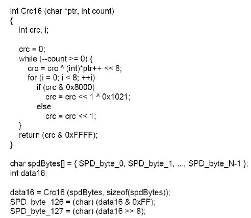
(When CST EZ-SPD
Programmer is used: The CST tester
automatically
calculates the CRC for you based on information of Byte 0 – Byte 125.)
Byte 128 – 255
Module Specific Section
This section of SPD bytes are specific to different families
DDR4
module. That is UDIMM, SO-DIMM, RDIMM, and LRDIMM as the common types
of Module. Module Type Byte 3 is used as an index for the encoding of
bytes 128 – 255. The content of bytes 128 – 255 are described in
multiple annexes, one for each memory module family.
Please refer to the annexes
session after Byte 383.
Byte 320
Module Manufacturer ID Code, Least Significant Byte
This code is obtained through manufacturer’s registration with
JEDEC
(the standard setting committee). A small fee is charged by JEDEC to
support and maintain this record. Please contact JEDEC office.
Byte 320 is the least significant byte. It is made up of the
number
of continuation codes + its parity. (See JEDEC JEP-106 for
“continuation codes”).
Example 1: Fujitsu’s continuation code is “0”. Therefore, Byte
320
Bits 0-6 is “0000000” while parity is “1”. That makes Byte 320 value
“10000000” = 80h.
Example 2: US Modular’s continuation code is “4”. Therefore,
Byte
320 Bits 0-6 is “0000100” while parity is “0”. That makes Byte 320
value “00000100” = 04h.
Byte 321
Module Manufacturer ID Code, Most Significant Byte
This code is obtained through manufacturer’s registration with
JEDEC
(the standard setting committee). A small fee is charged by JEDEC to
support and maintain this record. Please contact JEDEC office.
Byte 321 is the most significant byte. It represents the
Manufacturer’s registration code with JEDEC. (See JEDEC JEP-106 for
“Manufacturer codes”).
Example 1: Fujitsu’s Manufacturer code is “04”. Therefore,
Byte 321 Bits 0-7 is “00000100” = 04h.
Example 2: US Modular’s Manufacturer code is “A8”. Therefore,
Byte 321 Bits 0-7 is “10101000” =
A8h.
Byte 322
Module Manufacturing Location
Optional manufacturer assigned code.
Byte 323 - 324
Module Manufacturing Date
Byte 323 is for the year.
(When CST EZ-SPD
Programmer is used: User selects the year to
automatically enter the year code in hex.)
Byte 324 is for the week of the year, 1 to 52.
(When CST
EZ-SPD
Programmer is used: The program should automatically calculate the week
of the year once a day on the calendar is click selected and “OK” by
the user. It will also automatically convert to the proper SPD hex code)
Byte 325 - 328
Module Serial Number
Optional manufacturer assigned number.
On the Serial Number setting, JEDEC has no specification on
data
format nor dictates the location of the Most Significant Bit.
Therefore, it’s up to the individual manufacturer to assign his
numbering system.(All
CST testers and EZ-SPD programmers have the
option for the user to select either byte 325 or 328 as the MSB (most
significant bit). The tester assumes the use of ASCII format, which is
the most commonly used. The CST testers also have the function to
automatically increment the serial number on each module tested.)
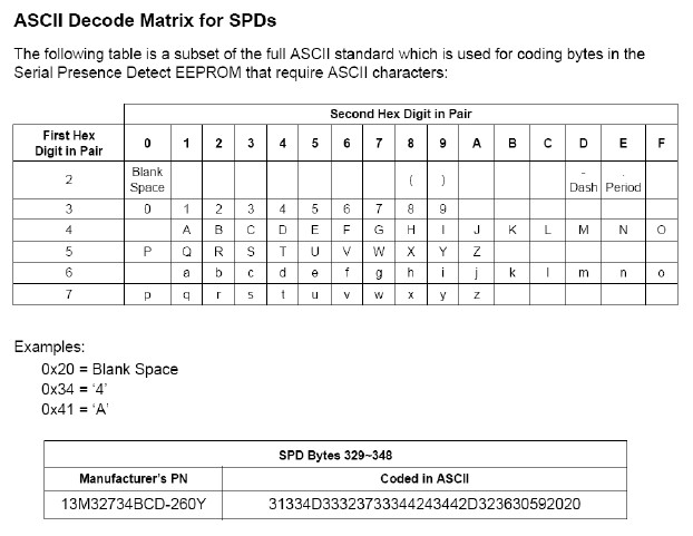
Byte 329 - 348
Module Part Number
The manufacturer’s part number is written in ASCII format
within these bytes.
Byte 329 is the most significant digit in ASCII while byte 348
is
the least significant digit in ASCII. Unused digits are coded as ASCII
blanks (20h).
(When CST EZ-SPD
Programmer is used: Simply click the button
at the
right of Byte 128 to open an edit window, input the manufacturer’s PN
(Maximum 18 digits). The software will automatically translate it into
ASCII and write them into Bytes 329 - 348.)
Byte 349
Module Revision Code
Optional Manufacturer Assigned Code. This revision code refers
to
the manufacturer’s assembly revision level and may be different than
the raw card revision in SPD byes 128 and 130.
Byte 350
DRAM Manufacturer ID Code, Least Significant Byte
This code is obtained through manufacturer’s registration with
JEDEC
(the standard setting committee). A small fee is charged by JEDEC to
support and maintain this record. Please contact JEDEC office.
Byte 350 is the least significant byte. It is made up of the
number
of continuation codes + its parity. (See JEDEC JEP-106 for
“continuation codes”).
Example 1: Samsung’s continuation code is “0”. Therefore, Byte
350
Bits 0-6 is “0000000” while parity is “1”. That makes Byte 350 value
“10000000” = 80h.
Example 2: Nanya’s continuation code is “3”. Therefore, Byte
350
Bits 0-6 is “0000011” while parity is “1”. That makes Byte 320 value
“10000011” = 83h.
Byte 351
DRAM Manufacturer ID Code, Most Significant Byte
This code is obtained through manufacturer’s registration with
JEDEC
(the standard setting committee). A small fee is charged by JEDEC to
support and maintain this record. Please contact JEDEC office.
Byte 351 is the most significant byte. It represents the
Manufacturer’s registration code with JEDEC. (See JEDEC JEP-106 for
“Manufacturer codes”).
Example 1: Samsung’s Manufacturer code is “CE”. Therefore,
Byte 351 Bits 0-7 is “11001110” =
CEh.
Example 2: Nanya’s Manufacturer code is “0B”. Therefore, Byte
351 Bits 0-7 is “00001010” =
0Bh.
Byte 352
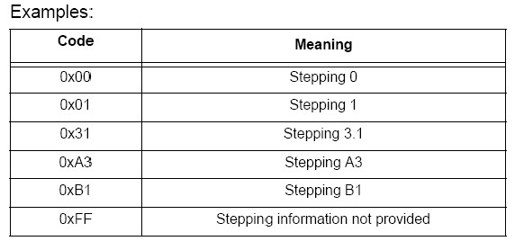
DRAM Stepping
This byte defines the vendor die revision level (often call
the
“stepping”) of the DRAM s on the module. This byte is optional. For
modules without DRAM stepping information, this byte should be
programmed to 0xFF.
Byte 353 -381
Manufacturer’s Specific Data
Optional manufacturer assigned code. The module manufacturer
may
include any additional information desired into the module within these
locations.
Byte 382: cyclical Redundancy Code (CRC) for
Manufacturer Section, LSB
Byte 383: cyclical Redundancy Code (CRC) for
Manufacturer Section, MSB
This two-byte field contains the calculated CRC for bytes 320
– 381
in the SPD. Also see SPD bytes 126 -127 for a coding example.
Annexes for
Byte 128 – Byte 255
Annex K.1
Covers
DDR4 UDIMM When Byte 2 =
0Ch Byte 3 = 02h
DDR4 SO-DIMM When Byte 2 = 0Ch Byte 3 =
03h
Byte 128 (Unbuffered) : Raw Card Extension, Module
Nominal Height
The Lower 5 bits of this byte define the nominal height (A
dimension) in millimeters of the fully assembled module including heat
spreaders or other added components. Refer to the relevant JEDEC JC-11
module outline (MO) documents for dimension definitions.
The upper 3 bits of this byte define revisions to the Raw Card
beyond revision 3. If the revision level is within 3, it is defined on
Byte 130, instead. Therefore, Bits 7-5 of Byte 128 is usually “000”
unless the revision level is higher than 3.
Module Nominal Height
|
Under or equal 15mm 00h
|
|
Between 15 and 16mm 01h
|
|
Between 16 and 17mm 02h
|
|
Between 17 and 18mm 03h
|
|
Between 18 and 19mm 04h
|
|
Between 19 and 20mm 05h
|
|
Between 20 and 21mm 06h
|
|
Between 21 and 22mm 07h
|
|
Between 22 and 23mm 08h
|
|
Between 23 and 24mm 09h
|
|
Between 24 and 25mm 0Ah
|
|
Between 25 and 26mm 0Bh
|
|
Between 26 and 27mm 0Ch
|
|
Between 27 and 28mm 0Dh
|
|
Between 28 and 29mm 0Eh
|
|
Between 29 and 30mm 0Fh
|
|
Between 30 and 31mm 10h
|
|
Between 31 and 32mm 11h
|
|
Between 32 and 33mm 12h
|
|
Between 33 and 34mm 13h
|
|
Between 34 and 35mm 14h
|
|
Between 35 and 36mm 15h
|
|
Between 36 and 37mm 16h
|
|
Between 37 and 38mm 17h
|
|
Between 38 and 39mm 18h
|
|
Between 39 and 40mm 19h
|
|
Between 40 and 41mm 1Ah
|
|
Between 41 and 42mm 1Bh
|
|
Between 42 and 43mm 1Ch
|
|
Between 43 and 44mm 1Dh
|
|
Between 44 and 45mm 1Eh
|
|
Over 45mm 1Fh
|
Byte 129 (Unbuffered): Module Maximum Thickness
This byte defines the maximum thickness in millimeters of the
fully
assembled module including heat spreaders and any other components. It
is in two parts; the front thickness (from PCB surface) and the back
thickness (from PCB surface).
(When CST EZ-SPD
Programmer is used: Simply selected by number
between 1-15mm for front thickness and by number between 1-15mm for
back thickness. Program automatically converts these thickness number
into 2 byte hex code.)
Example:
|
Smaller or equal to 1mm on both front and back 00h
|
|
1 to 2 mm on both front and back 11h
|
|
2 to 3 mm on both front and back 22h
|
|
3 to 4 mm on both front and back 33h
|
|
4 to 5 mm on both front and back 44h
|
|
5 to 6 mm on both front and back 55h
|
| |
|
2 mm on front 1 mm max on back 01h
|
|
3 mm on front 1 mm max on back 02h
|
|
4 mm on front 1 mm max on back 03h |
Byte 130 (Unbuffered): Reference Raw Card Used
This Byte indicates which JEDEC reference design raw card was
used
as the basis for the module assembly. It includes Raw Card designator
and Revision number.
(When CST EZ-SPD
Programmer is used: Simply select by number
on
revision code. Select Raw Card number by alphabetic code. Program
automatically calculates the 2 byte Hex number.)
|
Raw Card A rev. 0 00h , rev. 1 20h , rev. 2 40h , rev. 3
60h |
|
Raw Card B rev. 0 01h , rev. 1 21h , rev. 2 41h , rev. 3
61h
|
|
Raw Card C rev. 0 02h , rev. 1 22h , rev. 2 42h , rev. 3
62h
|
|
Raw Card D rev. 0 03h , rev. 1 23h , rev. 2 43h , rev. 3
63h
|
|
Raw Card E rev. 0 04h , rev. 1 24h , rev. 2 44h , rev. 3
64h
|
|
Raw Card F rev. 0 05h , rev. 1 25h , rev. 2 45h , rev. 3
65h
|
|
Raw Card G rev. 0 06h , rev. 1 26h , rev. 2 46h , rev. 3
66h
|
|
Raw Card H rev. 0 07h , rev. 1 27h , rev. 2 47h , rev. 3
67h
|
|
Raw Card J rev. 0 08h , rev. 1 28h , rev. 2 48h , rev. 3
68h
|
|
Raw Card K rev. 0 09h , rev. 1 29h , rev. 2 49h , rev. 3
69h
|
|
Raw Card L rev. 0 0Ah , rev. 1 2Ah , rev. 2 4Ah , rev. 3
6Ah
|
|
Raw Card M rev. 0 0Bh , rev. 1 2Bh , rev. 2 4Bh , rev. 3
6Bh
|
|
Raw Card N rev. 0 0Ch , rev. 1 2Ch , rev. 2 4Ch , rev. 3
6Ch
|
|
Raw Card P rev. 0 0Dh , rev. 1 2Dh , rev. 2 4Dh , rev. 3
6Dh
|
|
Raw Card R rev. 0 0Eh , rev. 1 2Eh , rev. 2 4Eh , rev. 3
6Eh
|
Raw Card T rev. 0 0Fh , rev. 1 2Fh , rev. 2 4Fh ,
rev. 3 6Fh
Raw Card U rev. 0 10h , rev. 1 30h , rev. 2 50h , rev. 3 70h
Raw Card V rev. 0 11h , rev. 1 31h , rev. 2 51h , rev. 3 71h
Raw Card W
rev. 0 12h , rev. 1 32h , rev. 2 52h , rev. 3 72h
Raw Card Y rev. 0 13h
, rev. 1 33h , rev. 2 53h , rev. 3 73h |
|
Raw Card AA rev. 0 14h , rev. 1 34h , rev. 2 54h , rev.
3 74h |
|
Raw Card AB rev. 0 15h , rev. 1 35h , rev. 2 55h , rev.
3 75h
|
|
Raw Card AC rev. 0 16h , rev. 1 36h , rev. 2 56h , rev.
3 76h
|
|
Raw Card AD rev. 0 17h , rev. 1 37h , rev. 2 57h , rev.
3 77h
|
|
Raw Card AE rev. 0 18h , rev. 1 38h , rev. 2 58h , rev.
3 78h
|
|
Raw Card AF rev. 0 19h , rev. 1 39h , rev. 2 59h , rev.
3 79h
|
|
Raw Card AG rev. 0 1Ah , rev. 1 3Ah , rev. 2 5Ah , rev.
3 7Ah
|
|
Raw Card AH rev. 0 1Bh , rev. 1 3Bh , rev. 2 5Bh , rev.
3 7Bh
|
|
Raw Card AJ rev. 0 1Ch , rev. 1 3Ch , rev. 2 5Ch , rev.
3 7Ch
|
|
Raw Card AK rev. 0 1Dh , rev. 1 3Dh , rev. 2 5Dh , rev.
3 7Dh
|
|
Raw Card AL rev. 0 1Eh , rev. 1 3Eh , rev. 2 5Eh , rev.
3 7Eh
|
| |
|
Raw Card AM rev. 0 80h , rev. 1 A0h , rev. 2 C0h , rev.
3 E)h |
|
Raw Card AN rev. 0 81h , rev. 1 A1h , rev. 2 C1h , rev.
3 E1h
|
|
Raw Card AP rev. 0 82h , rev. 1 A2h , rev. 2 C2h , rev.
3 E2h
|
|
Raw Card AR rev. 0 83h , rev. 1 A3h , rev. 2 C3h , rev.
3 E3h
|
|
Raw Card AT rev. 0 84h , rev. 1 A4h , rev. 2 C4h , rev.
3 E4h
|
|
Raw Card AU rev. 0 85h , rev. 1 A5h , rev. 2 C5h , rev.
3 E5h
|
|
Raw Card AV rev. 0 86h , rev. 1 A6h , rev. 2 C6h , rev.
3 E6h
|
|
Raw Card AW rev. 0 87h , rev. 1 A7h , rev. 2 C7h , rev.
3 E7h
|
|
Raw Card AY rev. 0 88h , rev. 1 A8h , rev. 2 C8h , rev.
3 E8h
|
|
Raw Card BA rev. 0 89h , rev. 1 A9h , rev. 2 C9h , rev.
3 E9h
|
|
Raw Card BB rev. 0 8Ah , rev. 1 AAh , rev. 2 CAh , rev.
3 EAh
|
|
Raw Card BC rev. 0 8Bh , rev. 1 ABh , rev. 2 CBh , rev.
3 EBh |
|
Raw Card BD rev. 0 8Ch , rev. 1 ACh , rev. 2 CCh , rev.
3 ECh
|
|
Raw Card BE rev. 0 8Dh , rev. 1 ADh , rev. 2 CDh , rev.
3 EDh
|
|
Raw Card BF rev. 0 8Eh , rev. 1 AEh , rev. 2 CEh , rev.
3 EEh
|
|
Raw Card BG rev. 0 8Fh , rev. 1 AFh , rev. 2 CFh , rev.
3 EFh
|
|
Raw Card BH rev. 0 90h , rev. 1 B0h , rev. 2 D0h , rev.
3 F0h
|
|
Raw Card BJ rev. 0 91h , rev. 1 B1h , rev. 2 D1h , rev.
3 F1h
|
|
Raw Card BK rev. 0 92h , rev. 1 B2h , rev. 2 D2h , rev.
3 F2h
|
|
Raw Card BL rev. 0 93h , rev. 1 B3h , rev. 2 D3h , rev.
3 F3h
|
|
Raw Card BM rev. 0 94h , rev. 1 B4h , rev. 2 D4h , rev.
3 F4h
|
|
Raw Card BN rev. 0 95h , rev. 1 B5h , rev. 2 D5h , rev.
3 F5h
|
|
Raw Card BP rev. 0 96h , rev. 1 B6h , rev. 2 D6h , rev.
3 F6h |
|
Raw Card BR rev. 0 97h , rev. 1 B7h , rev. 2 D7h , rev.
3 F7h
|
|
Raw Card BT rev. 0 98h , rev. 1 B8h , rev. 2 D8h , rev.
3 F8h
|
|
Raw Card BU rev. 0 99h , rev. 1 B9h , rev. 2 D9h , rev.
3 F9h
|
|
Raw Card BV rev. 0 9Ah , rev. 1 BAh , rev. 2 DAh , rev.
3 FAh
|
|
Raw Card BW rev. 0 9Bh , rev. 1 BBh , rev. 2 DBh , rev.
3 FBh
|
|
Raw Card BY rev. 0 9Ch , rev. 1 BCh , rev. 2 DCh , rev.
3 FCh
|
|
Raw Card CA rev. 0 9Dh , rev. 1 BDh , rev. 2 DDh , rev.
3 FDh
|
|
Raw Card CB rev. 0 9Eh , rev. 1 BEh , rev. 2 DEh , rev.
3 FEh
|
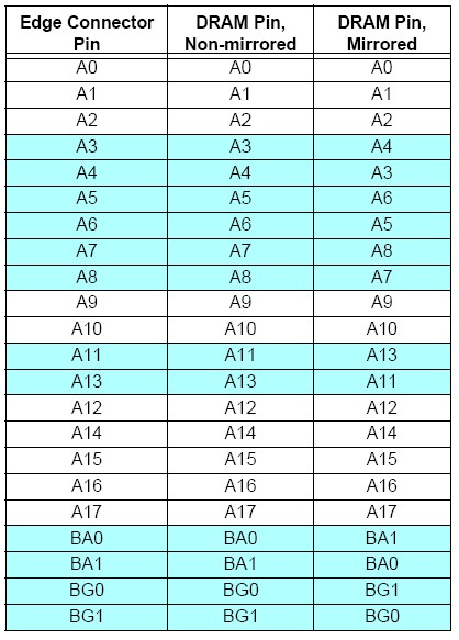
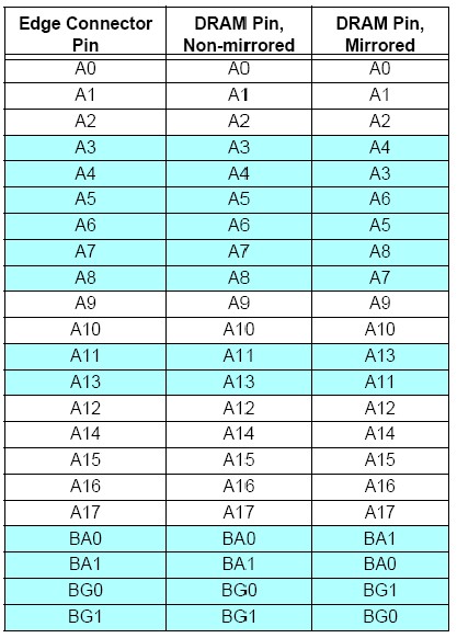
Byte 131 (Unbuffered): Address Mapping from Edge
Connector to DRAM
For ease of module PCB layout, sometimes “mirror” address
mapping is
used. “Mirror” address is to flip the address line sequence on the Even
rank of the module. This byte describes the connection of edge
connector pins for address bits to the corresponding input pins of the
DDR4 SDRAMs.
Rank 1
Mapping Standard 00h
Mirrored 01h
The definition of standard and mirrored address connection
mapping
is detailed below; highlighted rows in table indicate which signals
change between mappings.
Bytes 132 – 253 (Unbuffered):
Reserved must be coded 00h
Byte 254 (Unbuffered) : Cyclical Redundancy Code
(CRC) for Module Specific Section, LSB
Byte 254 (Unbuffered) : Cyclical Redundancy Code
(CRC) for Module Specific Section, LSB
This two-byte field contains the calculated CRC for bytes 128
– 253 in the SPD. See 126 – 127 for a coding example.
Annexes for
Byte 128 – Byte 255
Annex
K.2 Covers DDR4 RDIMM When Byte 2 =
0Ch Byte 3 = 01h
Byte 128 (Registered) : Raw Card Extension, Module
Nominal Height
The Lower 5 bits of this byte define the nominal height (A
dimension) in millimeters of the fully assembled module including heat
spreaders or other added components. Refer to the relevant JEDEC JC-11
module outline (MO) documents for dimension definitions.
The upper 3 bits of this byte define revisions to the Raw Card
beyond revision 3. If the revision level is within 3, it is defined on
Byte 130, instead. Therefore, Bits 7-5 of Byte 128 is usually “000”
unless the revision level is higher than 3.
Module Nominal Height
|
Under or equal 15mm 00h
|
|
Between 15 and 16mm 01h
|
|
Between 16 and 17mm 02h
|
|
Between 17 and 18mm 03h
|
|
Between 18 and 19mm 04h
|
|
Between 19 and 20mm 05h
|
|
Between 20 and 21mm 06h
|
|
Between 21 and 22mm 07h
|
|
Between 22 and 23mm 08h
|
|
Between 23 and 24mm 09h
|
|
Between 24 and 25mm 0Ah
|
|
Between 25 and 26mm 0Bh
|
|
Between 26 and 27mm 0Ch
|
|
Between 27 and 28mm 0Dh
|
|
Between 28 and 29mm 0Eh
|
|
Between 29 and 30mm 0Fh
|
|
Between 30 and 31mm 10h
|
|
Between 31 and 32mm 11h
|
|
Between 32 and 33mm 12h
|
|
Between 33 and 34mm 13h
|
|
Between 34 and 35mm 14h
|
|
Between 35 and 36mm 15h
|
|
Between 36 and 37mm 16h
|
|
Between 37 and 38mm 17h
|
|
Between 38 and 39mm 18h
|
|
Between 39 and 40mm 19h
|
|
Between 40 and 41mm 1Ah
|
|
Between 41 and 42mm 1Bh
|
|
Between 42 and 43mm 1Ch
|
|
Between 43 and 44mm 1Dh
|
|
Between 44 and 45mm 1Eh
|
|
Over 45mm 1Fh
|
Byte 129 (Registered): Module Maximum Thickness
This byte defines the maximum thickness in millimeters of the
fully
assembled module including heat spreaders and any other components. It
is in two parts; the front thickness (from PCB surface) and the back
thickness (from PCB surface).
(When CST EZ-SPD
Programmer is used: Simply selected by number
between 1-15mm for front thickness and by number between 1-15mm for
back thickness. Program automatically converts these thickness number
into 2 byte hex code.)
Example:
|
Smaller or equal to 1mm on both front and back 00h
|
|
1 to 2 mm on both front and back 11h
|
|
2 to 3 mm on both front and back 22h
|
|
3 to 4 mm on both front and back 33h
|
|
4 to 5 mm on both front and back 44h
|
|
5 to 6 mm on both front and back 55h
|
| |
|
2 mm on front 1 mm max on back 01h
|
|
3 mm on front 1 mm max on back 02h
|
|
4 mm on front 1 mm max on back 03h |
Byte 130 (Registered): Reference Raw Card Used
This Byte indicates which JEDEC reference design raw card was
used
as the basis for the module assembly. It includes Raw Card designator
and Revision number.
(When CST EZ-SPD Programmer is used: Simply select by number
on
revision code. Select Raw Card number by alphabetic code. Program
automatically calculates the 2 byte Hex number.)
|
Raw Card A rev. 0 00h , rev. 1 20h , rev. 2 40h , rev. 3
60h |
|
Raw Card B rev. 0 01h , rev. 1 21h , rev. 2 41h , rev. 3
61h
|
|
Raw Card C rev. 0 02h , rev. 1 22h , rev. 2 42h , rev. 3
62h
|
|
Raw Card D rev. 0 03h , rev. 1 23h , rev. 2 43h , rev. 3
63h
|
|
Raw Card E rev. 0 04h , rev. 1 24h , rev. 2 44h , rev. 3
64h
|
|
Raw Card F rev. 0 05h , rev. 1 25h , rev. 2 45h , rev. 3
65h
|
|
Raw Card G rev. 0 06h , rev. 1 26h , rev. 2 46h , rev. 3
66h
|
|
Raw Card H rev. 0 07h , rev. 1 27h , rev. 2 47h , rev. 3
67h
|
|
Raw Card J rev. 0 08h , rev. 1 28h , rev. 2 48h , rev. 3
68h
|
|
Raw Card K rev. 0 09h , rev. 1 29h , rev. 2 49h , rev. 3
69h
|
|
Raw Card L rev. 0 0Ah , rev. 1 2Ah , rev. 2 4Ah , rev. 3
6Ah
|
|
Raw Card M rev. 0 0Bh , rev. 1 2Bh , rev. 2 4Bh , rev. 3
6Bh
|
|
Raw Card N rev. 0 0Ch , rev. 1 2Ch , rev. 2 4Ch , rev. 3
6Ch
|
|
Raw Card P rev. 0 0Dh , rev. 1 2Dh , rev. 2 4Dh , rev. 3
6Dh
|
|
Raw Card R rev. 0 0Eh , rev. 1 2Eh , rev. 2 4Eh , rev. 3
6Eh
|
Raw Card T rev. 0 0Fh , rev. 1 2Fh , rev. 2 4Fh ,
rev. 3 6Fh
Raw Card U rev. 0 10h , rev. 1 30h , rev. 2 50h , rev. 3 70h
Raw Card V rev. 0 11h , rev. 1 31h , rev. 2 51h , rev. 3 71h
Raw Card W
rev. 0 12h , rev. 1 32h , rev. 2 52h , rev. 3 72h
Raw Card Y rev. 0 13h
, rev. 1 33h , rev. 2 53h , rev. 3 73h |
|
Raw Card AA rev. 0 14h , rev. 1 34h , rev. 2 54h , rev.
3 74h |
|
Raw Card AB rev. 0 15h , rev. 1 35h , rev. 2 55h , rev.
3 75h
|
|
Raw Card AC rev. 0 16h , rev. 1 36h , rev. 2 56h , rev.
3 76h
|
|
Raw Card AD rev. 0 17h , rev. 1 37h , rev. 2 57h , rev.
3 77h
|
|
Raw Card AE rev. 0 18h , rev. 1 38h , rev. 2 58h , rev.
3 78h
|
|
Raw Card AF rev. 0 19h , rev. 1 39h , rev. 2 59h , rev.
3 79h
|
|
Raw Card AG rev. 0 1Ah , rev. 1 3Ah , rev. 2 5Ah , rev.
3 7Ah
|
|
Raw Card AH rev. 0 1Bh , rev. 1 3Bh , rev. 2 5Bh , rev.
3 7Bh
|
|
Raw Card AJ rev. 0 1Ch , rev. 1 3Ch , rev. 2 5Ch , rev.
3 7Ch
|
|
Raw Card AK rev. 0 1Dh , rev. 1 3Dh , rev. 2 5Dh , rev.
3 7Dh
|
|
Raw Card AL rev. 0 1Eh , rev. 1 3Eh , rev. 2 5Eh , rev.
3 7Eh
|
| |
|
Raw Card AM rev. 0 80h , rev. 1 A0h , rev. 2 C0h , rev.
3 E)h |
|
Raw Card AN rev. 0 81h , rev. 1 A1h , rev. 2 C1h , rev.
3 E1h
|
|
Raw Card AP rev. 0 82h , rev. 1 A2h , rev. 2 C2h , rev.
3 E2h
|
|
Raw Card AR rev. 0 83h , rev. 1 A3h , rev. 2 C3h , rev.
3 E3h
|
|
Raw Card AT rev. 0 84h , rev. 1 A4h , rev. 2 C4h , rev.
3 E4h
|
|
Raw Card AU rev. 0 85h , rev. 1 A5h , rev. 2 C5h , rev.
3 E5h
|
|
Raw Card AV rev. 0 86h , rev. 1 A6h , rev. 2 C6h , rev.
3 E6h
|
|
Raw Card AW rev. 0 87h , rev. 1 A7h , rev. 2 C7h , rev.
3 E7h
|
|
Raw Card AY rev. 0 88h , rev. 1 A8h , rev. 2 C8h , rev.
3 E8h
|
|
Raw Card BA rev. 0 89h , rev. 1 A9h , rev. 2 C9h , rev.
3 E9h
|
|
Raw Card BB rev. 0 8Ah , rev. 1 AAh , rev. 2 CAh , rev.
3 EAh
|
|
Raw Card BC rev. 0 8Bh , rev. 1 ABh , rev. 2 CBh , rev.
3 EBh |
|
Raw Card BD rev. 0 8Ch , rev. 1 ACh , rev. 2 CCh , rev.
3 ECh
|
|
Raw Card BE rev. 0 8Dh , rev. 1 ADh , rev. 2 CDh , rev.
3 EDh
|
|
Raw Card BF rev. 0 8Eh , rev. 1 AEh , rev. 2 CEh , rev.
3 EEh
|
|
Raw Card BG rev. 0 8Fh , rev. 1 AFh , rev. 2 CFh , rev.
3 EFh
|
|
Raw Card BH rev. 0 90h , rev. 1 B0h , rev. 2 D0h , rev.
3 F0h
|
|
Raw Card BJ rev. 0 91h , rev. 1 B1h , rev. 2 D1h , rev.
3 F1h
|
|
Raw Card BK rev. 0 92h , rev. 1 B2h , rev. 2 D2h , rev.
3 F2h
|
|
Raw Card BL rev. 0 93h , rev. 1 B3h , rev. 2 D3h , rev.
3 F3h
|
|
Raw Card BM rev. 0 94h , rev. 1 B4h , rev. 2 D4h , rev.
3 F4h
|
|
Raw Card BN rev. 0 95h , rev. 1 B5h , rev. 2 D5h , rev.
3 F5h
|
|
Raw Card BP rev. 0 96h , rev. 1 B6h , rev. 2 D6h , rev.
3 F6h |
|
Raw Card BR rev. 0 97h , rev. 1 B7h , rev. 2 D7h , rev.
3 F7h
|
|
Raw Card BT rev. 0 98h , rev. 1 B8h , rev. 2 D8h , rev.
3 F8h
|
|
Raw Card BU rev. 0 99h , rev. 1 B9h , rev. 2 D9h , rev.
3 F9h
|
|
Raw Card BV rev. 0 9Ah , rev. 1 BAh , rev. 2 DAh , rev.
3 FAh
|
|
Raw Card BW rev. 0 9Bh , rev. 1 BBh , rev. 2 DBh , rev.
3 FBh
|
|
Raw Card BY rev. 0 9Ch , rev. 1 BCh , rev. 2 DCh , rev.
3 FCh
|
|
Raw Card CA rev. 0 9Dh , rev. 1 BDh , rev. 2 DDh , rev.
3 FDh
|
|
Raw Card CB rev. 0 9Eh , rev. 1 BEh , rev. 2 DEh , rev.
3 FEh
|
Byte 131 (Registered): DIMM Module Attributes
This byte indicates number of registers used on a module.
Further it
indicates number of rows of DRAM packages (monolithic, DDP or other
stacked) parallel to edge connector (independent of DRAM orientation)
on each side of the printed circuit board.
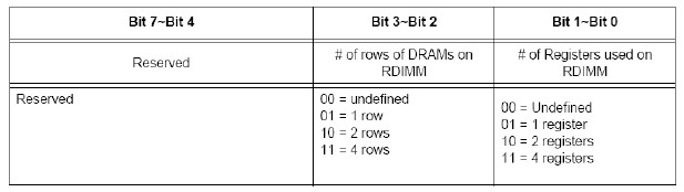
For Example:
1. A Registered module with attributes undefined = 00h
2. A Registered module with 2 rows of chips (either single,
DDP, or stacked) and 2 registers is (0000 1010) = 0Ah
Byte 132 (Registered): RDIMM Thermal Heat Spreader
Solution
This byte describes the module’s supported thermal heat
spreader solution.
Heat spreader solution not incorporated 00h
Heat spreader solution incorporated 80h
Byte 133 (Registered): Register Manufacturer ID Code,
Least Significant Byte
Byte 134 (Registered): Register Manufacturer ID Code,
Most Significant Byte
This two-byte field indicates the manufacturer of the register
used
on the module, encoded as follows: the first byte is the number of
continuation bytes indicated in JEP-106; the second byte is the last
non-zero byte of the manufacturer’s ID code, again as indicated in
JEP-106. These bytes are optional. For modules without the Register
Manufacturer ID code information, both bytes should be programmed to
00h.
Examples:
Inphi Corporation Byte 133 = 04h Byte 134 = B3h
Montage Technology Byte 133 = 86h Byte 134 = 32h
Integrated Device Technology (IDT) Byte 133 = 80h Byte 134 =
B3h
Byte 135 (Registered): Register Revision Number
This byte defines the vendor die revision level of the
registering
clock driver component. This byte is optional. For modules without the
Register Revision Number information, this byte should be programmed
FFh.
Examples:
Revision 0 00h
Revision 1 01h
Revision 3.1 31h
Revision A3 A3h
Revision B1 B1h
Byte 136 (Registered): Address Mapping from Register
to DRAM
This byte describes the connection of register output pins for
address bits to the corresponding input pins of the DDR4 SDRAMs for
rank 1 and rank 3 only; rank 0 and rank 2 are always assumed to use
standard mapping. Only two connection types are supported, standard or
mirrored, as described in the mapping table below.
Rank 1 Mapping
Standard 00h
Mirrored 01h
The definition of standard and mirrored address connection
mapping
is detailed below; highlighted rows in table indicate which signals
change between mappings.
Byte 137 (Registered): Register Output Drive Strength
for Control
This bye defines the drive strength for the registering clock
driver outputs.
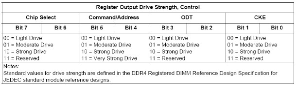
Example:
Chip select is using Moderate Drive 01
Command/Address are using Moderate Drive 01
ODT is using Strong Drive 10
CKE is using Moderate Drive 01
Therefore, the word is 01011001 = 59h
Byte 138 (Registered): Register Output Drive Strength
for CK
This byte defines the drive strength for the registering clock
driver outputs.
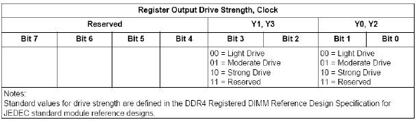
Example:
All differential clocks are in Strong Drive mode 0000 10 10 =
0Ah
Bytes TBD – 253 (Registered):
These bytes are Reserved and must be coded as 00h
Byte 254 (Registered): Cyclical Redundancy Code (CRC)
for Module specific Section, LSB.
Byte 254 (Registered): Cyclical Redundancy Code (CRC)
for Module specific Section, MSB.
This two-byte field contains the calculated CRC for bytes 128
– 253 in the SPD. See bytes 126 -127 for a coding example.
Annexes for
Byte 128 – Byte 255
Annex K.3
Covers DDR4 Load ReductionMemory Module
(LRDIMM)
When Byte 2 = 0Ch Byte 3 = 04h
Byte 128 (Load Reduced) : Raw Card Extension, Module
Nominal Height
The Lower 5 bits of this byte define the nominal height (A
dimension) in millimeters of the fully assembled module including heat
spreaders or other added components. Refer to the relevant JEDEC JC-11
module outline (MO) documents for dimension definitions.
The upper 3 bits of this byte define revisions to the Raw Card
beyond revision 3. If the revision level is within 3, it is defined on
Byte 130, instead. Therefore, Bits 7-5 of Byte 128 is usually “000”
unless the revision level is higher than 3.
Module Nominal Height
|
Under or equal 15mm 00h
|
|
Between 15 and 16mm 01h
|
|
Between 16 and 17mm 02h
|
|
Between 17 and 18mm 03h
|
|
Between 18 and 19mm 04h
|
|
Between 19 and 20mm 05h
|
|
Between 20 and 21mm 06h
|
|
Between 21 and 22mm 07h
|
|
Between 22 and 23mm 08h
|
|
Between 23 and 24mm 09h
|
|
Between 24 and 25mm 0Ah
|
|
Between 25 and 26mm 0Bh
|
|
Between 26 and 27mm 0Ch
|
|
Between 27 and 28mm 0Dh
|
|
Between 28 and 29mm 0Eh
|
|
Between 29 and 30mm 0Fh
|
|
Between 30 and 31mm 10h
|
|
Between 31 and 32mm 11h
|
|
Between 32 and 33mm 12h
|
|
Between 33 and 34mm 13h
|
|
Between 34 and 35mm 14h
|
|
Between 35 and 36mm 15h
|
|
Between 36 and 37mm 16h
|
|
Between 37 and 38mm 17h
|
|
Between 38 and 39mm 18h
|
|
Between 39 and 40mm 19h
|
|
Between 40 and 41mm 1Ah
|
|
Between 41 and 42mm 1Bh
|
|
Between 42 and 43mm 1Ch
|
|
Between 43 and 44mm 1Dh
|
|
Between 44 and 45mm 1Eh
|
|
Over 45mm 1Fh
|
Byte 129 (Load Reduced): Module Maximum Thickness
This byte defines the maximum thickness in millimeters of the
fully
assembled module including heat spreaders and any other components. It
is in two parts; the front thickness (from PCB surface) and the back
thickness (from PCB surface).
(When CST EZ-SPD
Programmer is used: Simply selected by number
between 1-15mm for front thickness and by number between 1-15mm for
back thickness. Program automatically converts these thickness number
into 2 byte hex code.)
Example:
|
Smaller or equal to 1mm on both front and back 00h
|
|
1 to 2 mm on both front and back 11h
|
|
2 to 3 mm on both front and back 22h
|
|
3 to 4 mm on both front and back 33h
|
|
4 to 5 mm on both front and back 44h
|
|
5 to 6 mm on both front and back 55h
|
| |
|
2 mm on front 1 mm max on back 01h
|
|
3 mm on front 1 mm max on back 02h
|
|
4 mm on front 1 mm max on back 03h |
Byte 130 (Load Reduced): Reference Raw Card Used
This Byte indicates which JEDEC reference design raw card was
used
as the basis for the module assembly. It includes Raw Card designator
and Revision number.
(When CST EZ-SPD
Programmer is used: Simply select by number
on
revision code. Select Raw Card number by alphabetic code. Program
automatically calculates the 2 byte Hex number.)
|
Raw Card A rev. 0 00h , rev. 1 20h , rev. 2 40h , rev. 3
60h |
|
Raw Card B rev. 0 01h , rev. 1 21h , rev. 2 41h , rev. 3
61h
|
|
Raw Card C rev. 0 02h , rev. 1 22h , rev. 2 42h , rev. 3
62h
|
|
Raw Card D rev. 0 03h , rev. 1 23h , rev. 2 43h , rev. 3
63h
|
|
Raw Card E rev. 0 04h , rev. 1 24h , rev. 2 44h , rev. 3
64h
|
|
Raw Card F rev. 0 05h , rev. 1 25h , rev. 2 45h , rev. 3
65h
|
|
Raw Card G rev. 0 06h , rev. 1 26h , rev. 2 46h , rev. 3
66h
|
|
Raw Card H rev. 0 07h , rev. 1 27h , rev. 2 47h , rev. 3
67h
|
|
Raw Card J rev. 0 08h , rev. 1 28h , rev. 2 48h , rev. 3
68h
|
|
Raw Card K rev. 0 09h , rev. 1 29h , rev. 2 49h , rev. 3
69h
|
|
Raw Card L rev. 0 0Ah , rev. 1 2Ah , rev. 2 4Ah , rev. 3
6Ah
|
|
Raw Card M rev. 0 0Bh , rev. 1 2Bh , rev. 2 4Bh , rev. 3
6Bh
|
|
Raw Card N rev. 0 0Ch , rev. 1 2Ch , rev. 2 4Ch , rev. 3
6Ch
|
|
Raw Card P rev. 0 0Dh , rev. 1 2Dh , rev. 2 4Dh , rev. 3
6Dh
|
|
Raw Card R rev. 0 0Eh , rev. 1 2Eh , rev. 2 4Eh , rev. 3
6Eh
|
Raw Card T rev. 0 0Fh , rev. 1 2Fh , rev. 2 4Fh ,
rev. 3 6Fh
Raw Card U rev. 0 10h , rev. 1 30h , rev. 2 50h , rev. 3 70h
Raw Card V rev. 0 11h , rev. 1 31h , rev. 2 51h , rev. 3 71h
Raw Card W
rev. 0 12h , rev. 1 32h , rev. 2 52h , rev. 3 72h
Raw Card Y rev. 0 13h
, rev. 1 33h , rev. 2 53h , rev. 3 73h |
|
Raw Card AA rev. 0 14h , rev. 1 34h , rev. 2 54h , rev.
3 74h |
|
Raw Card AB rev. 0 15h , rev. 1 35h , rev. 2 55h , rev.
3 75h
|
|
Raw Card AC rev. 0 16h , rev. 1 36h , rev. 2 56h , rev.
3 76h
|
|
Raw Card AD rev. 0 17h , rev. 1 37h , rev. 2 57h , rev.
3 77h
|
|
Raw Card AE rev. 0 18h , rev. 1 38h , rev. 2 58h , rev.
3 78h
|
|
Raw Card AF rev. 0 19h , rev. 1 39h , rev. 2 59h , rev.
3 79h
|
|
Raw Card AG rev. 0 1Ah , rev. 1 3Ah , rev. 2 5Ah , rev.
3 7Ah
|
|
Raw Card AH rev. 0 1Bh , rev. 1 3Bh , rev. 2 5Bh , rev.
3 7Bh
|
|
Raw Card AJ rev. 0 1Ch , rev. 1 3Ch , rev. 2 5Ch , rev.
3 7Ch
|
|
Raw Card AK rev. 0 1Dh , rev. 1 3Dh , rev. 2 5Dh , rev.
3 7Dh
|
|
Raw Card AL rev. 0 1Eh , rev. 1 3Eh , rev. 2 5Eh , rev.
3 7Eh
|
| |
|
Raw Card AM rev. 0 80h , rev. 1 A0h , rev. 2 C0h , rev.
3 E)h |
|
Raw Card AN rev. 0 81h , rev. 1 A1h , rev. 2 C1h , rev.
3 E1h
|
|
Raw Card AP rev. 0 82h , rev. 1 A2h , rev. 2 C2h , rev.
3 E2h
|
|
Raw Card AR rev. 0 83h , rev. 1 A3h , rev. 2 C3h , rev.
3 E3h
|
|
Raw Card AT rev. 0 84h , rev. 1 A4h , rev. 2 C4h , rev.
3 E4h
|
|
Raw Card AU rev. 0 85h , rev. 1 A5h , rev. 2 C5h , rev.
3 E5h
|
|
Raw Card AV rev. 0 86h , rev. 1 A6h , rev. 2 C6h , rev.
3 E6h
|
|
Raw Card AW rev. 0 87h , rev. 1 A7h , rev. 2 C7h , rev.
3 E7h
|
|
Raw Card AY rev. 0 88h , rev. 1 A8h , rev. 2 C8h , rev.
3 E8h
|
|
Raw Card BA rev. 0 89h , rev. 1 A9h , rev. 2 C9h , rev.
3 E9h
|
|
Raw Card BB rev. 0 8Ah , rev. 1 AAh , rev. 2 CAh , rev.
3 EAh
|
|
Raw Card BC rev. 0 8Bh , rev. 1 ABh , rev. 2 CBh , rev.
3 EBh |
|
Raw Card BD rev. 0 8Ch , rev. 1 ACh , rev. 2 CCh , rev.
3 ECh
|
|
Raw Card BE rev. 0 8Dh , rev. 1 ADh , rev. 2 CDh , rev.
3 EDh
|
|
Raw Card BF rev. 0 8Eh , rev. 1 AEh , rev. 2 CEh , rev.
3 EEh
|
|
Raw Card BG rev. 0 8Fh , rev. 1 AFh , rev. 2 CFh , rev.
3 EFh
|
|
Raw Card BH rev. 0 90h , rev. 1 B0h , rev. 2 D0h , rev.
3 F0h
|
|
Raw Card BJ rev. 0 91h , rev. 1 B1h , rev. 2 D1h , rev.
3 F1h
|
|
Raw Card BK rev. 0 92h , rev. 1 B2h , rev. 2 D2h , rev.
3 F2h
|
|
Raw Card BL rev. 0 93h , rev. 1 B3h , rev. 2 D3h , rev.
3 F3h
|
|
Raw Card BM rev. 0 94h , rev. 1 B4h , rev. 2 D4h , rev.
3 F4h
|
|
Raw Card BN rev. 0 95h , rev. 1 B5h , rev. 2 D5h , rev.
3 F5h
|
|
Raw Card BP rev. 0 96h , rev. 1 B6h , rev. 2 D6h , rev.
3 F6h |
|
Raw Card BR rev. 0 97h , rev. 1 B7h , rev. 2 D7h , rev.
3 F7h
|
|
Raw Card BT rev. 0 98h , rev. 1 B8h , rev. 2 D8h , rev.
3 F8h
|
|
Raw Card BU rev. 0 99h , rev. 1 B9h , rev. 2 D9h , rev.
3 F9h
|
|
Raw Card BV rev. 0 9Ah , rev. 1 BAh , rev. 2 DAh , rev.
3 FAh
|
|
Raw Card BW rev. 0 9Bh , rev. 1 BBh , rev. 2 DBh , rev.
3 FBh
|
|
Raw Card BY rev. 0 9Ch , rev. 1 BCh , rev. 2 DCh , rev.
3 FCh
|
|
Raw Card CA rev. 0 9Dh , rev. 1 BDh , rev. 2 DDh , rev.
3 FDh
|
|
Raw Card CB rev. 0 9Eh , rev. 1 BEh , rev. 2 DEh , rev.
3 FEh
|
Byte 131 (Load Reduced): DIMM Module Attributes
This byte indicates number of registers used on a module.
Further it
indicates number of rows of DRAM packages (monolithic, DDP or
3Dstacked) parallel to edge connector (independent of DRAM orientation)
on each side of the printed circuit board.
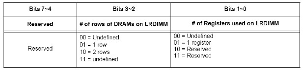
For Example:
1. A Load Reduced module with attributes undefined = 00h
2. A Load Reduced module with 2 rows of chips (either single,
DDP, or stacked) and 2 registers is (0000 1010) = 0Ah
Byte 132 (Load Reduced): LRDIMM Thermal Heat Spreader
Solution
This byte describes the module’s supported thermal heat
spreader solution.
Heat spreader solution not incorporated 00h
Heat spreader solution incorporated 80h
Byte 133 (Load Reduced): Register and Data Buffer
Manufacturer ID Code, Least Significant Byte
Byte 134 (Load Reduced): Register and Data Buffer
Manufacturer ID Code, Most Significant Byte
This two-byte field indicates the manufacturer of the memory
buffer
used on the module, encoded as follows: the first byte is the number of
continuation bytes indicated in JEP-106; the second byte is the last
non-zero byte of the manufacturer’s ID code, again as indicated in
JEP-106. These bytes are optional. For modules without the Register
Manufacturer ID code information, both bytes should be programmed to
00h.
Examples:
Inphi Corporation Byte 133 = 04h
Byte 134 = B3h
Montage Technology Byte 133 = 86h
Byte 134 = 32h
Integrated Device Technology (IDT) Byte 133 = 80h Byte 134 =
B3h
Byte 135 (Load Reduced): Register Revision Number
This byte defines the vendor die revision level of the
registering
clock driver component. For modules without the Register Revision
Number information, this byte should be programmed FFh.
Examples:
Revision 0 00h
Revision 1 01h
Revision 3.1 31h
Revision A3 A3h
Revision B1 B1h
Byte 136 (Load Reduced): Address Mapping from
Register to DRAM
This byte describes the connection of register output pins for
address bits to the corresponding input pins of the DDR4 SDRAMs for
rank 1 and rank 3 only; rank 0 and rank 2 are always assumed to use
standard mapping. Only two connection types are supported, standard or
mirrored, as described in the mapping table below.
Rank 1 Mapping
Standard 00h
Mirrored 01h
The definition of standard and mirrored address connection
mapping
is detailed below; highlighted rows in table indicate which signals
change between mappings.
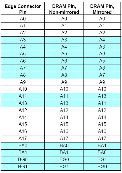
Byte 137 (Load Reduced): Register Output Drive
Strength for Control and Command/Address
This bye defines the drive strength for the registering clock
driver outputs.
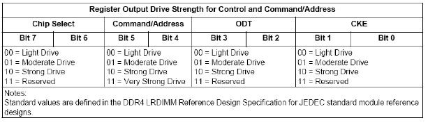
Example:
Chip select is using Moderate Drive 01
Command/Address are using Moderate Drive 01
ODT is using Strong Drive 10
CKE is using Moderate Drive 01
Therefore, the word is 01011001 =
59h
Byte 138 (Load Reduced): Register Output Drive
Strength for CK
This byte defines the drive strength for the registering clock
driver outputs.
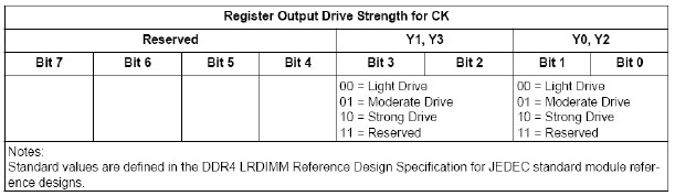
Example:
All differential clocks are in Strong Drive mode 0000 10 10 =
0Ah
Byte 139 (Load Reduced): Data Buffer Revision Number
This byte defines the vendor die revision level of the data
buffer
component. For modules without the Data Buffer Revision Number
information, this byte should be programmed FFh.
Examples:
Revision 0 00h
Revision 1 01h
Revision 3.1 31h
Revision A3 A3h
Revision B1 B1h
Byte 140 (Load Reduced): DRAM VrefDQ for Package Rank
0
This byte defines the VrefDQ value for the package rank 0
DRAMs.
On LRDIMM, the memory buffer re-drives the DQ lines to the
particular rank of DRAM on the module. The DRAM reference voltage has
to be trained to realize the optimum operation. This SPD byte tells the
system the range of values to set the initial VrefDQ for training.
Since the rising edge and the falling edge are asymmetrical, two ranges
have to be considered. This setting is through MR6 A5 – A0 encoding.
VrefDQ Training Values
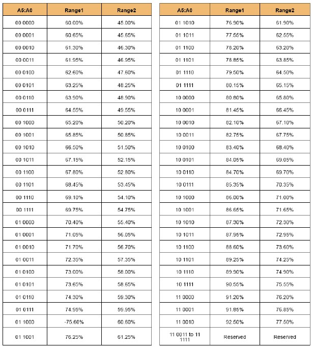
Examples:
1. The initial VrefDQ training range is from 60% of VDD to 45%
of VDD, A5 – A0 is 00 0000.
The byte is, therefore, 0000 0000 = 00h.
2. The initial VrefDQ training range is from 68.45% of VDD to
53.45%
of VDD, A5 – A0 is 00 1101. The byte is, therefore, 00001101 = 0Dh
3. The initial VrefDQ training range is from 91.85% of VDD
to76.85%
of VDD, A5 – A0 is 11 0001. The byte is, therefore, 0011 0001 = 31h
Byte 141 (Load Reduced): DRAM VrefDQ for Package Rank
1
This byte defines the VrefDQ value for the package rank 1
DRAMs.
Method and selection is similar to Byte 140 except for the
different rank.
Byte 142 (Load Reduced): DRAM VrefDQ for Package Rank
2
This byte defines the VrefDQ value for the package rank 2
DRAMs.
Method and selection is similar to Byte 140 except for the
different rank.
Byte 143 (Load Reduced): DRAM VrefDQ for Package Rank
3
This byte defines the VrefDQ value for the package rank 3
DRAMs.
Method and selection is similar to Byte 140 except for the
different rank.
Byte 144 (Load Reduced): Data Buffer VrefDQ for DRAM
Interface
This byte defines the DRAM Interface VrefDQ value for the data
buffer component.
Method and selection is similar to Byte 140.
F5BCX: DRAM Interface VREF Control word definition
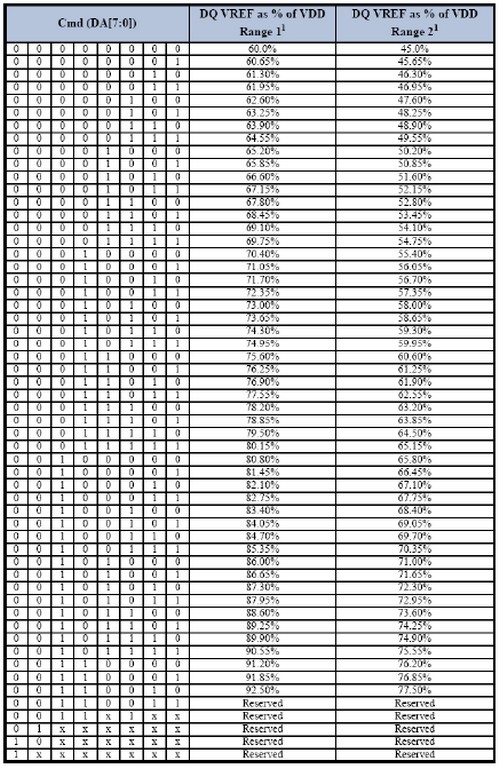
Byte 145 (Load Reduced): Data Buffer MDQ Drive
Strength and RTT for data rate ≤1866
This Byte defines the drive strength for MDQ/MDQS outputs and
the Read RTT termination strength of the data buffer component.
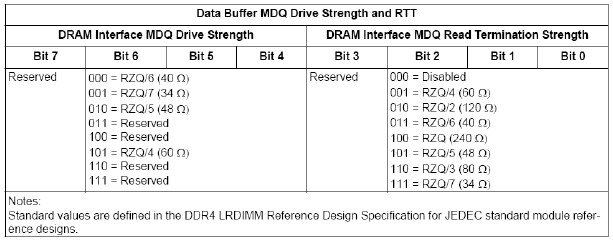
Example:
1. For MDQ Drive Strength = RZQ/5 (48Ω), MDQ Read Termination
Strength = RZQ/6 (40Ω) at data rate ≤ 1866 Byte 145 = 0010 0011 = 23h
2. For MDQ Drive Strength = RZQ/6 (40Ω), MDQ Read Termination
Strength = RZQ/4 (60Ω) at data rate ≤ 1866 Byte 145 = 0000 0001 = 01h
Byte 146 (Load Reduced): Data Buffer MDQ Drive
Strength and RTT for 1866 < data rate ≤ 2400
This Byte defines the drive strength for MDQ/MDQS outputs and
the Read RTT termination strength of the data buffer component.
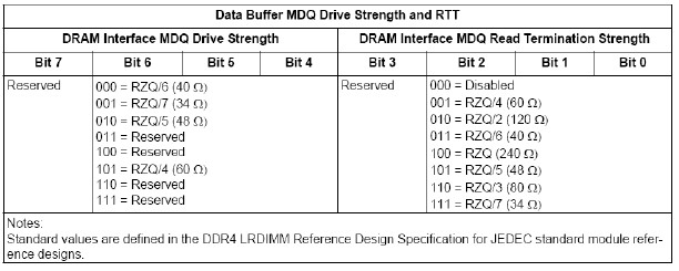
Example:
1. For MDQ Drive Strength = RZQ/5 (48Ω), MDQ Read Termination
Strength = RZQ/6 (40Ω) at 1866 < data rate ≤ 2400Byte 146 = 0010
0011 = 23h
2. For MDQ Drive Strength = RZQ/6 (40Ω), MDQ Read Termination
Strength = RZQ/4 (60Ω) at 1866 < data rate ≤ 2400Byte 146 = 0000
0001 = 01h
Byte 147 (Load Reduced): Data Buffer MDQ Drive
Strength and RTT for 2400 < data rate ≤ 3200
This Byte defines the drive strength for MDQ/MDQS outputs and
the Read RTT termination strength of the data buffer component.
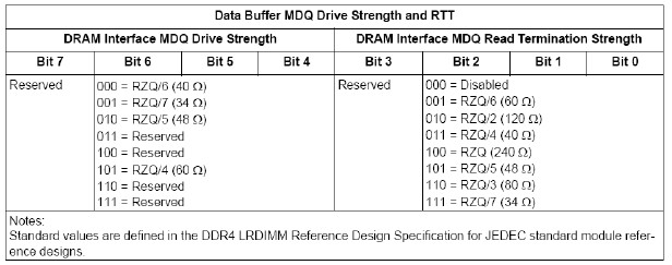
Example:
1. For MDQ Drive Strength = RZQ/5 (48Ω), MDQ Read Termination
Strength = RZQ/6 (60Ω) at2400 < data rate ≤ 3200 Byte 147 = 0010
0001 = 21h
2. For MDQ Drive Strength = RZQ/6 (40Ω), MDQ Read Termination
Strength = RZQ/4 (40Ω) at2400 < data rate ≤ 3200 Byte 147 = 0000
0011 = 03h
Byte 148 (Load Reduced): DRAM Drive Strength (for
data rate ≤ 1866, 1866 < data rate ≤ 2400, and 2400 <
data rate ≤ 3200)
This Byte defines the output buffer drive strength for the
DRAMs.
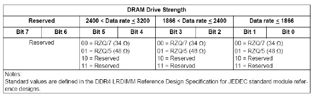
Example:
1. 2400
2. 2400
Byte 149 (Load Reduced): DRAM ODT (RTT_WR and
RTT_NOM) for data rate ≤ 1866
This Byte defines the ODT termination strength for the DRAMs.
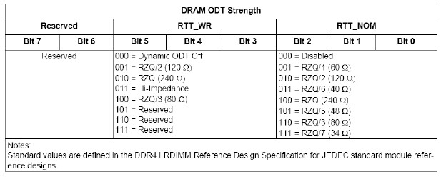
Example:
1. For RTT_WR Drive Strength = 120Ω, RTT_NOM Strength = 60Ω at
data rate ≤ 1866 Byte 149 = 0000 1001 = 09h
2. For RTT_WR Drive Strength = 80Ω, RTT_NOM Strength = 40Ω at
data rate ≤ 1866 Byte 149 = 0010 0011 = 23h
Byte 150 (Load Reduced): DRAM ODT (RTT_WR and
RTT_NOM) for 1866 < data rate ≤ 2400
This Byte defines the ODT termination strength for the DRAMs.
Example:
1. For RTT_WR Drive Strength = 120Ω, RTT_NOM Strength = 60Ω at
1866 < data rate ≤ 2400 Byte 150 = 0000 1001 = 09h
2. For RTT_WR Drive Strength = 80Ω, RTT_NOM Strength = 40Ω at
1866 < data rate ≤ 2400 Byte 150 = 0010 0011 = 23h
Byte 151 (Load Reduced): DRAM ODT (RTT_WR and
RTT_NOM) for 2400 < data rate ≤ 3200
This Byte defines the ODT termination strength for the DRAMs.

Example:
1. For RTT_WR Drive Strength = 120Ω, RTT_NOM Strength = 60Ω at
2400 < data rate ≤ 3200 Byte 151 = 0000 1001 = 09h
2. For RTT_WR Drive Strength = 80Ω, RTT_NOM Strength = 40Ω at
2400 < data rate ≤ 3200 Byte 151 = 0010 0011 = 23h
Byte 152 (Load Reduced): DRAM ODT (RTT_PARK) for data
rate ≤ 1866
This Byte defines the ODT termination strength for the DRAMs
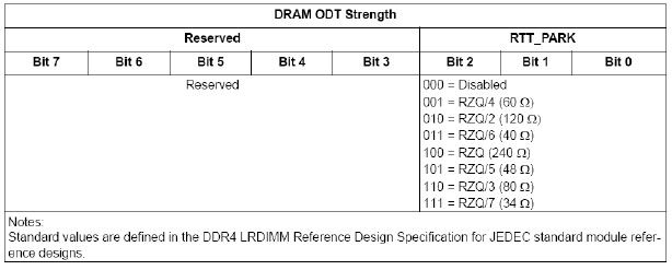 . .
Example:
1. For RTT_PARK Drive Strength = 60Ω, at data rate ≤ 1866 Byte
152 = 0000 0001 = 01h
2. For RTT_PARK Drive Strength = 120Ω, at data rate ≤ 1866
Byte 152 = 0000 0010 = 02h
Byte 153 (Load Reduced): DRAM ODT (RTT_PARK) for 1866
< data rate ≤ 2400
This Byte defines the ODT termination strength for the DRAMs.

Example:
1. For RTT_PARK Drive Strength = 60Ω, at 1866 < data
rate ≤ 2400 Byte 153 = 0000 0001 = 01h
2. For RTT_PARK Drive Strength = 120Ω, at 1866 < data
rate ≤ 2400 Byte 153 = 0000 0010 = 02h
Byte 154 (Load Reduced): DRAM ODT (RTT_PARK) for 2400
< data rate ≤ 3200
This Byte defines the ODT termination strength for the DRAMs.
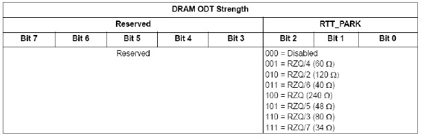
Example:
1. For RTT_PARK Drive Strength = 60Ω, at 2400 < data
rate ≤ 3200 Byte 154 = 0000 0001 = 01h
2. For RTT_PARK Drive Strength = 120Ω, at 2400 < data
rate ≤ 3200 Byte 154 = 0000 0010 = 02h
Bytes 155 – 253 (Load Reduced):
Reserved – must be coded 00h
Byte 254 (Load Reduced): Cyclical Redundancy Code
(CRC) for Module specific Section, LSB.
Byte 254 (Load Reduced): Cyclical Redundancy Code
(CRC) for Module specific Section, MSB.
This two-byte field contains the calculated CRC for bytes 128
– 253 in the SPD. See bytes 126 -127 for a coding example.
Final Note:
This Article is presently based on JEDEC DDR4 DIMM
SPD Specification V0.7
Major difference between DDR4 and DDR3 are:
1. EEPROM size has been increased to 512 bytes. Actual used
bytes are 384 bytes.
2. SPD codes are divided into 3 sections: Byte 0 – 127, Byte
128 – 255, and Byte 256 – 383.
3. Each of the 3 sections has their own 2 bytes of SPD
sectional CRC.
4. Different Module Type has their own differentiated SPD
table
annex on Byte 125 – 255. There are differentiations between
UDIMM/SODIMM (Annex K1), RDIMM (Annex K2), and LRDIMM (Annex K3).
Everything in the above
article and more are now implemented
into the CST EZ-SPD DDR4 Programmer software. The features are:
1. Pop up window of explanation on each Byte.
2. Clickable selection right from the illustration window.
3. Auto CRC checksum on byte 126/127, byte 254/255, and byte
382/383.
4. Text input on "manufacturer code" and "serial number". User
define MSB/LSB format.
5. Auto JEDEC week and year coding
from PC clock.
6. Reversible Software write protect function.
.....just to name a few.
For further information, please view : www.simmtester.com
By: DocMemory
Copyright © 2023 CST, Inc. All Rights Reserved
|