Monday, March 18, 2013
JEDEC Solid State Technology Association announced the initial publication of its widely anticipated DDR4 SDRAM standard, JESD79-4, the voluminous document described the DDR4 SDRAM device in exacting detail.
However, JESD79-4 was not intended as a tutorial on system design or to provide explanations as to if and how specific system designs should be migrated to utilize DDR4 SDRAM devices, so it’s left to the readers to imagine the possible advantages of the technology at the system level. Consequently, a knowledge gap exists between the presentation of the technical details in JESD79-4 and understanding the underlying motivations and rationale that led to the standard. In an attempt to bridge that knowledge gap, let’s explain some of the purpose of the DDR4 SDRAM device, and frame it in the context of system level trends.[1] By understanding the underlying motivations of the DDR4 SDRAM device specification, engineers and program managers can better decide whether or not their current and future designs should migrate to support DDR4 SDRAM devices.
The DDR4 SDRAM device is an evolutionary device that improves upon the DDR3 SDRAM generation in terms of capacity, performance scalability, power efficiency, as well as system-level reliability, availability and serviceability (RAS). At the same time, DDR4 must minimize changes that hinder design migration and adoption of the new industry-standard component.
Let’s explore the distinctions between DDR3 and DDR4, how the latter enhances system-level capacity and performance scalability, and DDR4’s various innovations that improve power efficiency. Then we’ll look at the various techniques designed into a DDR4 SDRAM device that improve system-level RAS. Finally, we’ll address the challenges of migrating DDR3 memory systems to DDR4 SDRAM.
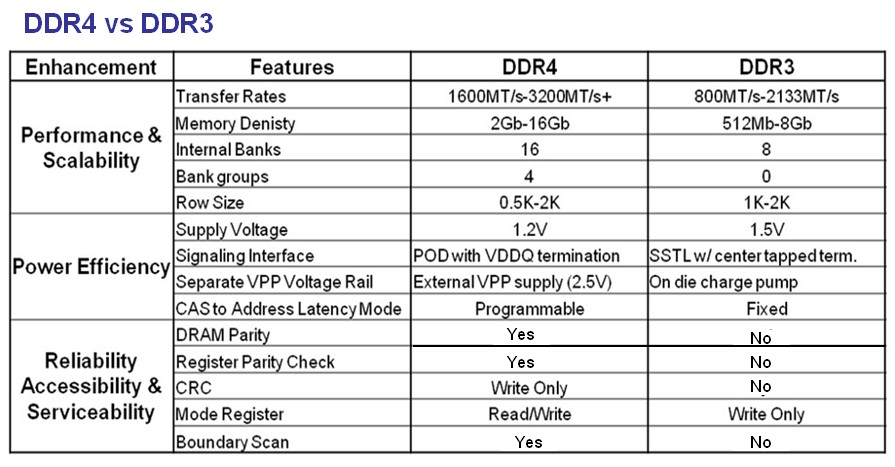
Improved capacity and performance scalability
One subtle and yet important difference that distinguishes the two is that DDR4 is organized differently from DDR3—specifically in the area of how DDR4 is designed to support high-speed multi-core processors. The 8-Gb DDR4 SDRAM device with 4-bit-wide data bus interface (x4), for example, is internally organized as a device with four bank groups and four banks in each bank group. Within each bank in the 8-Gb x4 DDR4 SDRAM device, there are 131,072 (217) rows, with 512 bytes of DRAM cells per row. Compared to the 8-Gb x4 DDR3 SDRAM device, which has eight independent banks, 65536 (216) rows per bank, and 2048 bytes per row, the 8-Gb x4 DDR4 SDRAM device has more banks.[2] Moreover, the 8-Gb x4 DDR4 SDRAM device has significantly smaller row sizes than the 8-Gb x4 DDR3 SDRAM device, meaning that the 8-Gb x4 DDR4 SDRAM device can cycle through different banks at a far higher rate than could the 8-Gb x4 DDR3 SDRAM device.[3]
A comparison of a DDR3 LRDIMM to a DDR4 RDIMM shows that the largest DDR3 SDRAM module may be constructed with quad die packages (QDP) of 8Gb x4 DRAM devices, reaching a theoretical maximum capacity of 128GB for a single-memory module (see figure 1). Figure 1 also shows that a DDR4 RDIMM may be constructed with upwards of eight-high DRAM stacks[5], supporting a theoretical maximum capacity of 512 GB per module. Furthermore, this diagram illustrates that the pin count on the DDR4 memory module has been increased to 284 pins, to support the higher addressing capability, as well as a 1:1 signal-to-ground ratio for the data bus (DQ) interface signals. Overall, figure highlights a few of the component and module-level changes that enable the DDR4 memory module to simultaneously support higher capacity and higher performance than the DDR3 memory module.
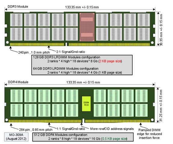
Figure 1: Comparison of a DDR4 SDRAM module (bottom) to a DDR3 SDRAM module (top) shows the increased pin count for DDR4 memory modules, the decreased pitch, and the 1:1 signal-to-ground ratio for the data bus interface signals.
Improved power efficiency
Another major area that the DDR4 SDRAM specification targeted for improvement over the DDR3 SDRAM specification is in the area of power efficiency. Aside from further reducing the DRAM I/O voltage (VDDQ) from 1.35 V used by DDR3L DRAM devices to 1.2 V, the DDR4 SDRAM device also specifies that a separate VPP voltage supply be provided to support high DRAM core word line voltage requirements[6]. The data I/O electrical interface signaling has been changed from series-stub terminated logic (SSTL) to pseudo-open drain (POD). A comparison of DDR3-style SSTL signaling to DDR4-style POD signaling highlights how the output driver drives electrical high, and the SSTL circuit incurs the cost of the I2 drive current, as well as the I1 termination current due to the center tapped termination (CTT).
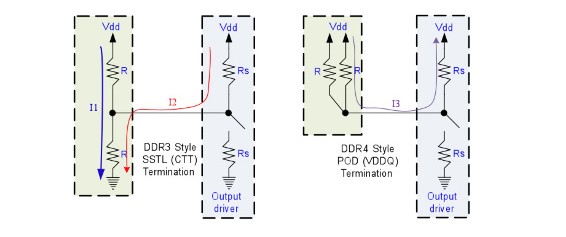
Figure 2: The DDR3 output driver drives the electrical high and the SSTL circuit incurs the cost of the I2 drive current, as well as the I1 termination current due to the center tapped termination (CTT), while POD signaling of DDR4 incurs no current flow in the case of driving electrical high, allowing reducing the DDR4 power requirements.
In contrast, the DDR4-style POD signaling incurs no current flow in the case of driving electrical high.[7] Collectively, the reduced VDDQ voltage, the use of VPP supply for boosted word line voltage, the change to POD signaling and VDDQ termination, and the previously discussed smaller row sizes that reduce activation currents lead to significant reductions in power consumption for DDR4 when compared to DDR3 SDRAM. Preliminary analysis suggests that at comparable operating data rates, a DDR4 SDRAM device has a 30% advantage in power efficiency compared to a DDR3 SDARM device.[8] That improvement can be used to operate the DDR4 SDRAM device at higher speeds, thus attaining higher performance or reduced power consumption at comparable performance levels.
Improved reliability, availability and serviceability (RAS)
Another area that the DDR4 SDRAM device specification targeted for improvement is in the area of RAS. One example in which the DDR4 SDRAM specification improves RAS is that DDR4 device supports command and address parity error detection, as well as recovery from parity error. A second example is that the DDR4 device supports a connectivity test mode, so that a system controller can test and detect connectivity faults without needing to go through DRAM initialization sequencing. Additionally, the DDR4 register also provides enhanced RAS over the DDR3 register in that the DDR4 register can be configured to support command blocking upon detection of a parity error; that is, in the case of a command and address parity error, the DDR3 register passes the erroneous command to the DRAM devices, making error recovery difficult. In contrast, the DDR4 register blocks the erroneous command and the DDR4 SDRAM device never sees the erroneous commands in the case of address parity error, thereby reducing the complexity of the error recovery process. Additionally, the DDR4 SDRAM device specification includes some optional features such as cyclic redundancy check (CRC) protection for write data to further enhance RAS. The extensive feature set ensures that as the DDR4 SDRAM device scales further in frequency where error rates may be non-negligible, future memory systems can take advantage of the enhanced RAS features in the DDR4 SDRAM device to improve the robustness of the memory system. This enables not just error detection but also capabilities to report and recover from multiple types of errors.
The JESD79-4 specification for DDR4 SDRAM devices ushered in numerous evolutionary improvements over DDR3 SDRAM devices. The DDR4 SDRAM device and the DDR4 memory module still rely on the same single-ended signaling and system infrastructure requirements, as do DDR3 SDRAM memory systems. Various changes have been made to device organization to better facilitate migration to multi-core systems and multi-threaded applications. In essence, the various JEDEC member companies utilized the in-field learning experiences of DDR3 SDRAM memory systems, enhanced performance and capacity scaling, and significantly improved system-level RAS, while attaining improved power efficiency.
With smaller rows and better power efficiency leading to performance and power advantages, DDR4 memory devices should see broad adoption in multi-core server and workstation systems starting in 2014. Thereafter, as 8-Gb DRAM begins to see widespread adoption, DDR4 SDRAM devices should then become the dominant commodity memory type and enjoy a cost-per-bit advantage, in addition to the aforementioned performance and power advantages.
Designers looking to maximize performance, power, RAS and cost-sensitive systems in next-generation servers should evaluate using DDR4 SDRAM devices as the memory type of choice.
Prototype DDR4 DIMM SODIMM Memory Module Tester
Designers looking to for DDR4 memory module test solutions will not have to wait too long. CST a memory module tester manufacturers will offer a complete DDR4 DIMM/SODIMM Test solutions by Q4 , 2013. For more information on DDR4 memory testing, check on www.simmtester.com for more informations.
By: DocMemory
Copyright © 2023 CST, Inc. All Rights Reserved
|

