Monday, April 5, 2010
Determine Endurance on a NAND Flash Chip
Introduction
What is “endurance” on a NAND Flash chip? The answer can be vague and inconclusive. Generally, the ballpark number on an SLC device (Single Level Cell) is 100,000 cycles while for MLC (Multi-Level Cell) is 10,000 cycles. To grasp the real picture, we should first look into the functional physic behind the NAND device and also understand how does it work?
 What is a NAND Memory? What is a NAND Memory?
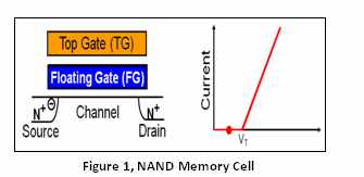
Let’s look at a simple FET transistor with Gate, Drain and Source. When a voltage (Vt) is applied to the Gate, the Gate is charged. At a certain point, electron moves down to the Drain/Source level to bridge the Drain and Source. The transistor is switched on. Drain and Source will conduct. We call this a “1” output.
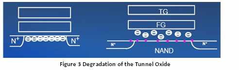
A NAND Flash transistor adds Floating Gate between the regular Gate and the Dain/Source. This Floating Gate retards the electron migration and thus changes the threshold voltage (Vt) the transistor would turn on. Programming the NAND means injecting electrons to the Floating Gate. High Threshold voltage pulls electrons up and electron quantum-mechanically tunneling through the “tunnel oxide” to form a “0”. Erase means removing electrons from the Floating Gate and tunnel in reverse direct. The gate would be stuck on as a “1”.
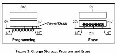
One program followed by an erase is call a “cycle”. As NAND is used, it can undergo many cycles. During these cycles, the transistor exerts harsh stress on the tunnel oxide with very high electric field. Al lot of electrons passes through the oxide. As a result, the oxide degrades. Atomic bonds in the oxide can be broken, both in the bulk and at the interface. Broken –bond sites can trap electrons that pass through, becoming electrically negative. Tunnel oxide degradation is the main reason why the number of cycles possible (or endurance) is finite.
When negative charges in tunnel oxide raises the Vt so programming gets faster and erase slower with cycling. When a block erases slower than datasheet, it fails and is retired. NAND datasheet allow 2% to 4% of blocks to fail in this way. When that % is reached, the device itself has failed.
 NAND Programming Structure NAND Programming Structure
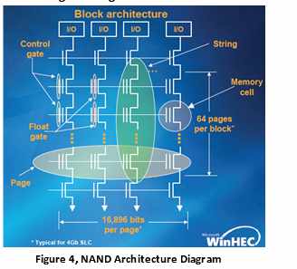
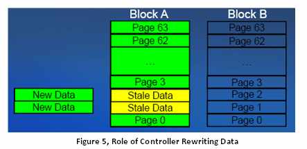
To simplify control architecture (see NAND architecture diagram), NAND program is in “page” unit, erase is in “block” unit. Therefore, suppose host wants to rewrite some data into a block, it cannot over-write directly. It needs to write the data to an erased block and then erase the original block. This can result into physically wrote 64 pages when host wrote only want to write 2 pages. This is call “amplification factor” of 32. Notice this will speed up the deterioration of the cells.
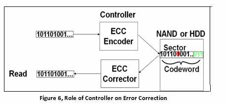
 System Controller Manages the NAND Operations System Controller Manages the NAND OperationsTo compensate for that in a NAND flash system software tricks are used in the controller. Basically, there are two main strategies. One is ECC (Error Correction Code). The system adds extra bits to the stored data organized in mathematical algorithm in relationship to the data. At the retrieval, the controller compare these extra bits and figure out the error bit and thus automatically correct and restore them.
The second strategy is “wear leveling” that automatically re-assign physical addresses on each write to make sure the usage is distributed among all the blocks in the system.
 Besides these two principle strategies, modern controller adds other hardware/software manipulations depending on the system operation environments. New algorithm and smarter systems are being invented everyday. With the system architect and correction strategy continue to evolve everyday, it will be impossible to put a definition on “NAND System Endurance”. However, if we narrow down the endurance to the NAND chip level, it would be much simpler. We can take the ECC, write leveling , and the controller out of the picture. Measuring NAND Chip Endurance
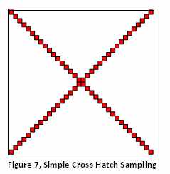
A typical 32Gbit NAND chip has 2048Kbyte to the Page and 64pages to the Block. Therefore, we can count 2048 X 8 X64 = 1048,576bits per block. The entire chip will have 32Gbit/1048kbits = 335536 blocks. If we take a sample of, say 1% of the blocks (336 block) and to test them, we would possibly able to determine by estimation the endurance of the entire chip. This would more be true if we would choose these 336 blocks from an even location distribution through out the chip. Initially we can choose address locations from a diagonal cross-hatch line on the chip (see diagram).
We would Erase and re-write the 336 blocks in a continuous cycle loop. At the same time, the status bit is monitored for failures. On a typical MLC NAND, the intrinsic cycle time is about :
Programming is 200usec. Per page X 64page per block = 0.0128sec. per block
Erase is 2msec. per block = 0.02sec. per block
Total cycle time for 336 blocks is therefore = 11.02sec. per 336blocks.
Estimated 10,000cycles will take only = 110,020sec. =30.81 hours
We see that this is still within reasonable test time of a little more than 1 day. With 1% bad cells, the remaining chip is still usable as a new chip. The worn out block would simply be masked as bad block by the system controller. This can be a straight forward and reasonable way to predict the “endurance” of a NAND chip. The tester is just have to have the capability to look at the failure status at each cycle to determine when the block under test has gone bad and became un-recoverable.
If the test go according to plan, cells on the tested block should start to fail at around 10,000 cycles (MLC). When all 312 selected blocks have all failed, we can average the fail cycle on the blocks to derive the estimated “endurance” of the rest of the cells on the chip.
Data Retention on NAND
On NAND Flash, there is another failure factor call “retention”. “Retention” is how long the cell would maintain its programmed state when the chip is not under power bias. This parameter is very sensitive and dependent on external environment. High temperature tends to reduce retention duration. Number of read cycles performed can also degrade this retention. Therefore, we must keep test temperature at about room temperature when testing NAND chip endurance.
Disclaimer
The endurance test method stated in this article is only one of the many ways to test for NAND chip endurance. There are many factors that can affect the endurance test result. The blogger solicit suggestions to continue enhance the test. Email discussions are welcome
By: DocMemory
Copyright © 2023 CST, Inc. All Rights Reserved
|