Friday, May 2, 2008
How to test DDR3 SODIMM and common test challenges ?
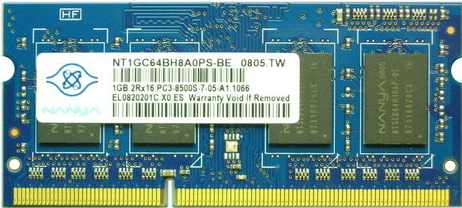
A typical 204pin DDR3 SODIMM manufacturerd by Nanya
DDR3 SODIMM modules will be used in the upcoming Intel Centrino-2 platform, also known as Montevina which is slated for Q3 released.
Samsung, Micron, Elpida, Qimonda and Hynix have all announced that its DDR3 SO-DIMM modules have been validated by Intel. The SODIMM modules operates at 800MHz and 1066MHz using latest process at 60nm.
All the Dram vendors have said they are ready with an entire line-up of DDR3 SODIMM modules for the new mobile platform, which brings full support for Intel's mobile 45nm processors.
Notebooks PC is able to achieve low-power consumption using low voltage of 1.5V. DDR3 SODIMM not only allows for higher system performance, but it also uses only 1.5V of power compared to DDR2’s 1.8V, thereby extending battery life by approximately 20 minutes. To further enhance performance per watt, DDR3 can also make use of an on-die heat sensor for improved thermal management.
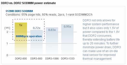
Typical Power saving : DDR3 SODIMM vs DDR2 SODIMM
To realize high-speed operation, DDR3 SO-DIMM employs component-level 8-bit pre-fetch and fly-by topology at the DIMM level to improve signal integrity.To avoid flight-time difference between DQ/DM/DQS signals and achieve high-speed operations the DDR3 system uses a de-skew mechanism to compensate for flight-time difference.
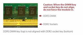
DDR3 SODIMM modules have the same form-factor as DDR2, but with 4 additional pins. They are also keyed differently to prevent accidental insertion into DDR2 sockets.
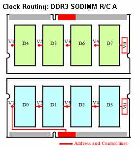
What is Fly-By Clock Routing?
Fly By Clock Scheme Different From Previous Generations
Let’s first examine the “Fly By” clock routing on a DDR3 DIMM. The clock routing (CK0) would hit D0 and then D1, D2, D3….D7 for the 1st Rank. The second Rank would be served by CK1 on routing sequence of D8, D9…..D15. In the desktop system, the mother board bios would do the leveling test to find out the appropriate delay it needs before capturing the data on the DQ lines. For example, it would capture DQ0-DQ7 as the first group and then DQ8-DQ15 as the second group with DQ56-DQ63 as the last group.
On the DDR3 SODIMM, the system approach is similar on Raw Card A,B, C, and D. D0 always start from the left side. Therefore, chip D0 is always the starting chip with the clock. However, it is different on Raw Card E and Raw Card F. Please see comparison pictures below.
*Note: The term Raw Card refers to the standard DIMM printed circuit board design published by JEDEC Standardization Committee. They are generally recognized as the reference design for memory modules. More infos on Raw cards can be found in www.jedec.org
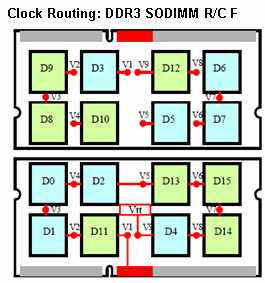
On DDR3 SODIMM R/C F, the clock starts at D11 and then D1, D0, D2…. This would totally upset the leveling sequence. The bios will have to know it is SODIMM R/C F to be able start out the leveling test and thus compensate for the difference in chip location sequence.
On the desktop motherboard, the bios is not programmed to recognize SODIMM R/C F and therefore would not know how to compensate for it. This is probably the main reason why the DDR3 R/C F SODIMM would not work on a desktop motherboard even with a proper converter.
DDR3 SODIMM Does Not Use Mirror Address ( Common Testing Challenges)
On DDR3 long DIMM (240pin), the address lines on Rank 2 is always “mirrored”. In order to make the DIMM module layout without cross address lines on a 2 rank module, it is good to have the DRAM chips on the back side to have flipped over address line sequence. Therefore, an option is built-in to the DDR3 DRAM chips to flip over its address. That is to make A0 the highest address and Axx as the lowest address. This way, the address pin out on the back side of the module would be exactly a mirror to the front side of the module.
However, on an SODIMM ( 204pin) design, back-to-back chip type of layout is not always practical. Mirror address on the second rank would not be very useful. Therefore, the “Mirror Address” method is not used on DDR3 SODIMM. Instead, address sequence on rank 2 would be “non-mirror”. Since a DIMM to SODIMM converter is just a socket wire interchange, it would not have accounted for the non-mirror address on the second rank. That is probably why most module manufacturer found out that SODIMM converters when used on a long DIMM motherboard would always detect only the first rank of memory.
Note : Motherboard will ignore the 2nd Rank if a DIMM-SODIMM Converter is used
The Available DDR3 SODIMM Test Solution
Well, the question is asked many times by the module manufacturers : What is the correct method for testing DDR3 SODIMM ?
CST, Inc. (www.simmtester.com), has created a test solution to allow the use of SODIMM converter on a standard long DIMM DDR3 tester. The CST SP3000-1066Mhz DDR3 tester detects a jumper signature on the SODIMM converter and switches itself to the SODIMM test mode automatically. It would automatically level out the timing difference caused by data sequence scrambling. It would also set the rank 2 address to “non-mirror” mode.
In summary, the CST DDR3 tester, with its clever design accommodates the testing of DDR3 long DIMM and SODIMM all in one unit. It takes the worry out of you, the memory module manufacturer.
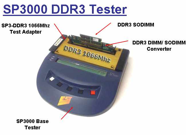
For information regarding the SP3000 DDR3 1066Mhz Tester Solution , contact : 972-2412662 or email info request to : info@simmtester.com
By: DocMemory
Copyright © 2023 CST, Inc. All Rights Reserved
|