|
 |
|

|
|
Memory Grades, the Most Confusing Subject
|
Monday, December 20, 1999
If you work in the PC industry, you probably have heard about EDO memory, SDRAM, PC100 and more recently PC133 and PC800 RDRAM. You may have seen –10, -8, -6 markings on SDRAM chips and wondered what they mean. You may have wondered if PC800 RDRAM is really 8 times faster than PC100 or how much faster is PC100 over EDO memory. In this article, we will compare how memory speed grade is defined for different types of technologies and hopeful de-mystify this confusing subject of memory grades. Due to its popularity as main memory in PC, this article covers only DRAM.
1. DRAM Fundamentals
Before we get into comparisons of individual memory technology, we first look at how DRAM works in general.
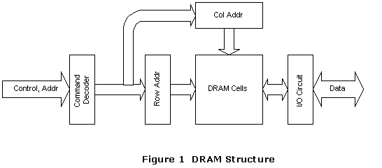
Internally DRAM has a huge array of cells that contain data. A pair of row and column addresses can uniquely address each cell in the DRAM. DRAM communicates with a memory controller through two main groups of signals: Control/Address signals and Data signals. The control signals tell the DRAM what operation is executed; the address signals tell the DRAM the cell location to perform the operation on and the data signals to transfer data to and from the DRAM.
In order to access a cell in DRAM, the following steps are necessary:
- A row command to latch in Row address
- A column command to latch in Column address
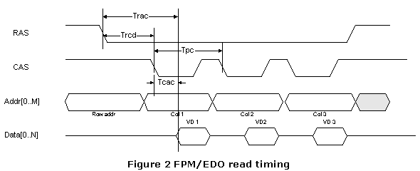
There is a necessary delay between the two commands as well as a delay after the column command for the I/O circuit to drive valid data. When we sum these two delays together we have the random access time of the DRAM. It is the minimum time it takes the memory controller to read data randomly from DRAM. Figure 2 illustrates this sequence in the first DRAM read cycle.
2. EDO/FPM Memory
Let’s now take a look at EDO and FPM memory. FPM stands for Fast-Page-Mode and EDO stands for Extended-Data-Out. EDO is enhanced FPM. EDO/FPM memory takes advantage of the fact that when cells within the same row are accessed, the row command doesn’t need to be repeated. The operation mode where multiple column commands follow a single row command is called Page Mode. Figure 2 provides graphic illustration of page mode access.
Let’s call the delay between a row command to a column command Trcd and the delay from column command to valid data Tcac. The random access time is Trac = Trcd + Tcac. (refer to Figure 2 for illustration diagram) Typically you would see –70, -60, -6, -5 or –50 marking on EDO/FPM DRAMs. These numbers refer to Trac = 70ns, 60ns and 50ns. Obviously the smaller the number the faster the DRAM.
In a PC, the memory access is often done in page mode. When L2 Cache is present in a PC, the page mode access rate is really the true indicator of the memory speed that determines system performance. Thus, random access time is not the best indicator for memory speed pertaining to system performance. Rather the page mode cycle time, Tpc indicates the peak data rate in FPM/EDO DRAM. EDO DRAM is almost identical to FPM except that data is turned off later in read mode. This difference allows EDO to have shorter Tpc, thus it increases system performance. For a –6 or –60 FPM DRAM, typically the Tpc = 35ns. For a –60 EDO DRAM typically the Tpc = 25ns. So for the same –60 part, EDO DRAM is about 30% faster than FPM DRAM in peak data rate.
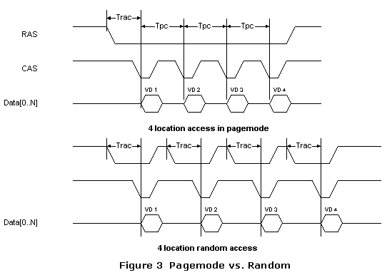
Let’s use an example to illustrate how page mode impacts the system performance.
- Scenario 1: 4 random memory accesses without page mode.
- Scenario2: 4 memory accesses in the same row with page mode.
We are assuming 70ns parts are used and using typical number of 40ns for page mode cycle. In scenario 1, the minimum total time needed to read 4 cells is 4xTrac=4x70 = 280ns. In scenario 2, only the first access takes full 70ns, the successive reads only take 40ns each. Thus, the total time needed to read 4 random cells in the same row is Trac+3xTpc=70+3x40 = 190ns. Page mode access is at least 32% faster. This is illustrated in Figure 3.
3. SDRAM, PC100 and PC133
There are two points from the discussion of EDO/FPM that needs to be highlighted here in the discussion about SDRAM. One is that in page mode, the column command can set random address within the row. The other one is that we noticed the page mode cycle time, Tpc is better indicator of memory performance than Trac, random access time. SDRAM specifically improved on both of these issues.
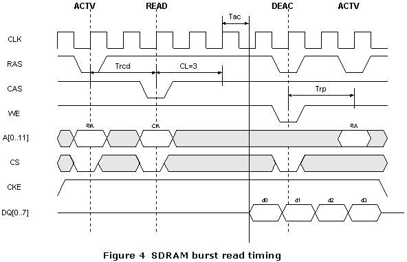
It is observed that instructions and data in the PC main memory tends to be read in sequential order most of the time. With the L2 Cache present, memory transactions happen as bursts of fixed sized memory block with continuous addresses. For example, in Pentium class CPU, 32 consecutive bytes in memory are transferred every time between the L2 Cache and main system memory. With these observations, DRAM designers come out with a better design called SDRAM which stands for Synchronous DRAM. SDRAM fixed the page mode address pattern to be sequential and introduced free running clock for all timing reference as well as page mode cycle indicator. The page mode access in SDRAM is called burst mode. Figure 4 shows SDRAM burst read timing.
3.1 Clock Cycle and Clock Frequency
Since burst mode has fixed address patterns, burst cycle time can be much shorter than that of page mode cycle. The clock cycle time of SDRAM is set to be the same as burst cycle time. Instead of random access time, the clock cycle time Tclk is used appropriately as the indicator of SDRAM speed. The –12, -10 –8 markings on the SDRAM chip usually indicates the minimum clock cycle time for the SDRAM component. A –12 marking means the clock cycle time for the SDRAM is 12ns.That in turn means the maximum clock frequency for the part is 83Mhz.
Typically some margin is given when ICs is mounted on a module, that is why module with –12 parts usually runs in 66Mhz systems. For the same reason, -8 parts (max frequency 125MHz) are used in 100Mhz system.
PC100 and PC133 refer to SDRAM module specifications for 100Mhz and 133Mhz PC systems. Roughly speaking, -8 parts or faster can be used for PC100 module, -6 or faster can be used for PC133 module. We have seen –75 (7.5ns clock cycle time) parts being used on modules labeled as PC133 as well. There is no standard way of marking SDRAM chips. For example, on some of the Samsung SDRAM chips there is no “-xx” marking, the user would have to decode the speed with a databook or goto the vendor’s website.
3.2 What is a 2-2-2 SDRAM?
Besides the clock frequency, other commonly used timing gauge for SDRAM are: Trp, Trcd and Tcl. They are marked in Figure 4.
Trp tells us how fast SDRAM can terminate one row access and starts another one.
Trcd definition is the same as FPM DRAM.
Tcl is known as "CAS latency".
Tcl determines which clock edge is access time measured from in SDRAM.
As indicated in Figure 4, Cas latency =3 means the access time Tac is measured from the 2nd clock edge after the "Read" command. All these parameters, Trp, Trcd and Tcl are expressed in number of clock cycles. If you have heard about a 2-2-2 100Mhz SDRAM, it is telling you the SDRAM can work at 100Mhz with Trp, Trcd and Tcl all equals to two clock cycles.
3.3 Access Time in SDRAM
The access time Tac for SDRAM is defined differently from EDO/FPM DRAM.
SDRAM access time is defined as access time in burst mode and is defined from certain clock edge (clock latency). Typical access time for PC100 SDRAM is about 7ns, but it does not mean PC100 SDRAM is 7 times faster than 50ns EDO DRAM. When we compare 7ns to 70ns, we are compare apples to oranges. In order to do a fair comparison, we need to convert the SDRAM access time to random access time.
Let’s do that for a PC100 SDRAM to see how much faster it is than a 50ns EDO DRAM. The Trcd for PC100 SDRAM is typically 2 clock cycles which is 20ns. Assuming a CAS latency of 2 and access time of 7ns. The random access time is 20+17 = 37ns. So a PC100 module is about as fast as a 40ns EDO module for random access. In burst mode, PC100 SDRAM is faster than a 40ns EDO DRAM.
4. PC800 RDRAM and PC266 DDR, which is faster?
The term PC800 and PC266 are kind of misleading because they only tell half of the fact.
PC800 is used by Intel and Rambus to indicate the 800Mhz peak data transfer rate for Direct Rambus memory technology. But Rambus module is only 2 bytes wide while SDRAM module is 8 bytes wide.
The formula for peak bandwidth is PBW = Peak_Data_Rate x Data_Bus_Width.
The peak bandwidth of PC800 Rambus module = 800Mhz x 2 Bytes = 1.6GB/s.
The peak bandwidth for PC100 SDRAM =100Mhz x 8 Bytes = 800MB/s, exactly half of the PC800 Rambus module.
PC266 DDR has a peak data transfer rate of 266Mhz and like SDRAM module, a DDR module has an 8 byte wide bus. Therefore,
the peak bandwidth for PC266 DDR is 266Mhz x 8 Bytes = 2.1GB/s, about 30% higher than PC800 RDRAM.
The actual system performance of a different memory technology is much more complicated than simply compare peek bandwidth.
This article is meant to give you some basic understanding of how different types of memory are graded.
By: Albert Lin
Copyright © 2023 CST, Inc. All Rights Reserved
|
|
|
|
